
Connectors Overview
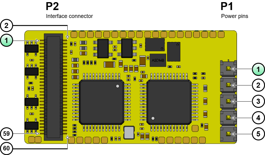
P1 Power pins
|
Gold plated 2.54 mm pitch pins. |
||||
|
# |
Signal name |
Type |
Description |
WARNING, POWER TERMINALS! |
|---|---|---|---|---|
|
1 |
GND |
Power
|
Power supply negative (Power Ground). Internally connected to GND_D. |
Power pins can have high voltages > 50 V, always respect clearance and creepage requirements (Typ > 0.25 mm)! Dimension PCB traces and connectors according to the current of the application! |
|
2 |
+VBUS |
Power supply positive (DC bus). |
||
|
3 |
PHASE_A |
Motor phase A for 3-phase motors, positive for DC / Voice coil motors. |
||
|
4 |
PHASE_B |
Motor phase B for 3-phase motors, negative for DC / Voice coil motors. |
||
|
5 |
PHASE_C |
Motor phase C for 3-phase motors (do not connect for DC motors). |
||
|
It is recommended to solder the power pins to reduce power losses. It also improves thermal performance by providing a preferential path for heat dissipation from the power stage to the environment. However, plugging and unplugging can be achieved by using a mating connector: MillMax 3305-0-15-15-47-27-10-0 socket. |
||||
P2 Interface connector
The connectors of DEN-S-NET are the same as DEN-NET, but the pinout has some minor modifications (indicated in yellow).
|
# |
Signal name |
Description |
Type |
# |
Signal name |
Description |
Type |
|---|---|---|---|---|---|---|---|
|
1 |
GND_D |
Digital signal Ground. |
Power |
2 |
GND_D |
Digital signal Ground. |
Power |
|
3 |
PHY1_TX_P |
Port 1 Ethernet physical layer differential pairs. 50 Ω pull-up termination resistors are included on the drive. Magnetics with the center tap connected to MAGNETICS_CT (pin 54) must be added externally. If this port is not used leave these pins unconnected. |
I/O |
4 |
3.3V_REF |
3.3 V ± 0.2% voltage reference output with sink/source capability up to ±10 mA. Excessive current demand or noise coupled to this pin can cause a loss of performance or even malfunction: route by following the best layout practices. |
Power output |
|
5 |
PHY1_TX_N |
6 |
AN1_OUT |
0.3 V to 3 V Analog output 1. Weak output, requires buffering. |
Analog output |
||
|
7 |
PHY1_RX_P |
8 |
AN1_P |
Analog input 1. Can be used as brake current sensing or for generic analog input. |
16 bit differential analog input |
||
|
9 |
PHY1_RX_N |
10 |
AN1_N |
||||
|
11 |
\ETH1_LED_LINK |
Ethernet Port 1 Link signaling. Can directly drive a (typically) green LED cathode by sinking up to 3 mA while the anode is connected to 3.3 V. |
Output |
12 |
AN2_P |
Analog input 2. Can be used as a brake current sensing or for generic analog input. |
16 bit differential analog input |
|
13 |
\SAFE_INPUT_1A |
Channel A of the redundant Safe Input 1. Active with low-level or open-circuit. Up to 7V voltage tolerant. Holding different logic states (\SAFE_INPUT_1A ≠ \SAFE_INPUT_1B) for more than 3.4s will cause a latching fault. |
Input |
14 |
AN2_N |
||
|
15 |
GND_D |
Digital signal Ground. |
Power |
16 |
MOTOR_TEMP |
Motor temperature sensor dedicated analog input. 0 to 3.3 V level high impedance input. The connection of the sensor should be done between GND_D and MOTOR_TEMP with a pull-up resistor (recommended value 1.65 kΩ) to 3.3V |
12 bit single-ended analog input |
|
17 |
\SAFE_INPUT_1B |
Channel B of the redundant Safe Input 1. Active with low-level or open-circuit. Up to 7V voltage tolerant. Holding different logic states (\SAFE_INPUT_1A ≠ \SAFE_INPUT_1B) for more than 3.4s will cause a latching fault. |
Input |
18 |
NC |
Not connected. |
|
|
19 |
DNC |
Reserved. Do not connect (leave floating). |
- |
20 |
NC |
Not connected. |
|
|
21 |
DNC |
Reserved. Do not connect (leave floating). |
- |
22 |
GPI1 |
Digital Input 1. |
Input |
|
23 |
3.3V_D |
3.3 V power supply input. Must be connected together to the pin 56. A well-regulated ±3%, low ripple, 1 A peak, 300 mA continuous source must be used (300 mA is total consumption shared between pin 23 and 56). 3.3 V power supply should have a rise time between 30 µs and 150 µs, and should be powered up before or together with 5V. |
Power input |
24 |
GPI2 |
Digital Input 2. |
Input |
|
25 |
NC |
Not Connected. |
- |
26 |
GPO1 |
Digital Output 1. |
Output |
|
27 |
5V_FBK_SENSE |
Analog input for sensing the Feedback Supply. See Safety Manual / Integration Requirements. |
Input |
28 |
GPO2 |
Digital Output 2. |
Output |
|
29 |
3.3V_SAFE |
3.3 V safe power supply output. This net is exclusive to power safety related circuits. Limited to 150 mA consumption. See Safety Manual / Integration Requirementss. |
Power output |
30 |
PWM_BRAKE |
PWM output for driving a mechanical brake. Configurable up to 40 kHz. A high level indicates the motor is free to move. |
Output |
|
31 |
GND_D |
Digital signal Ground. |
Power |
32 |
ABSENC1_DATA |
Data input for Absolute Encoder 1 (supports SSI or up to 2 BiSS-C encoders connected in daisy chain topology). |
Input |
|
33 |
3.3V_FBK_SENSE |
Not Connected. |
- |
34 |
ABSENC1_CLK |
Clock output for Absolute Encoder 1. Note: Keep the capacitance below 60 pF to maintain the clock signal integrity at frequencies up to 10 MHz |
Output |
|
35 |
\BOOT |
This pin can be pulled down to GND_D to force enter boot mode during power-up. Typically not necessary. If not used, always leave unconnected or pulled up with a 10 kΩ resistor. Never leave this pin permanently pulled down, as this would block the Denali boot mode. |
I/O |
36 |
GND_D |
Digital signal Ground. |
Power |
|
37 |
NC |
Not connected. |
|
38 |
ABSENC2_CLK |
Clock output for Absolute Encoder 2. |
Output |
|
39 |
NC |
Not Connected. |
- |
40 |
ABSENC2_DATA |
Data input for Absolute Encoder 2 (supports SSI or BiSS-C encoders). Note: Keep the capacitance below 60 pF to maintain the clock signal integrity at frequencies up to 10 MHz |
Input |
|
41 |
NC |
Not connected. |
|
42 |
DIG_ENC_1A |
Incremental encoder 1 A. |
Input, 3.3 V level single-ended. |
|
43 |
FAULT_SIGNAL |
Fault state signaling output. Can directly drive a (typically) red LED anode at 3.3 V up to 3 mA. |
Output |
44 |
DIG_ENC_1B |
Incremental encoder 1 B. |
|
|
45 |
ECAT_CAN_RUN |
State-machine RUN green LED output for EtherCAT and CANopen. Can directly drive a green LED anode at 3.3 V up to 3 mA. |
Output |
46 |
DIG_ENC_1Z |
Incremental encoder 1 Index. |
|
|
47 |
ECAT_CAN_ERR |
State machine ERROR red LED for EtherCAT and CANopen. Can directly drive a red LED anode at 3.3 V up to 3 mA. |
Output |
48 |
HALL_1 |
Digital hall 1. 0 to 3.3 V level high impedance input. Typical Hall sensor interface based on pull-up and schmitt trigger buffer should be provided on the interface board. |
Input, 3.3 V level single-ended |
|
49 |
\ETH0_LED_LINK |
Ethernet Port 0 Link signaling. Can directly drive a (typically) green LED cathode by sinking up to 3 mA while the anode is connected to 3.3 V. |
Output |
50 |
HALL_2 |
Digital hall 2. 0 to 3.3 V level high impedance input. Typical Hall sensor interface based on pull-up and schmitt trigger buffer should be provided on the interface board. |
|
|
51 |
PHY0_TX_P |
Port 0 Ethernet physical layer differential pairs. 50 Ω pull-up termination resistors are included on the drive. Magnetics with the center tap connected to MAGNETICS_CT (pin 54) must be added externally. If this port is not used leave these pins unconnected. |
I/O |
52 |
HALL_3 |
Digital hall 3. 0 to 3.3 V level high impedance input. Typical Hall sensor interface based on pull-up and schmitt trigger buffer should be provided on the interface board. |
|
|
53 |
PHY0_TX_N |
54 |
MAGNETICS_CT |
Supply input for the Ethernet PHY modules, which must also supply the magnetics center tap. Two voltages can be provided:
|
Power input |
||
|
55 |
PHY0_RX_P |
56 |
3.3V_D |
3.3 V power supply input. Must be connected together to the pin 23. A well-regulated ±3%, low ripple, 1 A peak, 300 mA continuous source must be used (300 mA is total consumption shared between pin 23 and 56). 3.3 V power supply should have a rise time between 30 µs and 150 µs, and should be powered up before or together with 5V. |
Power input |
||
|
57 |
PHY0_RX_N |
58 |
5V_D |
5 V logic power supply input. A well regulated ±3%, low ripple, 500 mA peak, 250 mA continuous source must be used. |
Power input |
||
|
59 |
GND_D |
Digital signal Ground. |
Power |
60 |
GND_D |
Digital signal Ground. |
Power |
Notes and naming conventions:
-
All pins are tolerant to 3.3 V unless otherwise noted.
-
Unused digital outputs should be left unconnected.
-
"_P" and "_N" indicate positive and negative terminals of differential signals
-
"\" Indicates inverted (active low) signal
-
"NC" means Not Connected. Pins marked with NC can be tied to GND or 3.3 V, but the best practice is to leave them unconnected.
-
"DNC" means Do Not Connect. Pins marked with DNC must not be tied to any driving voltage, including GND or 3.3 V.
Mating connector for P2 (Interface connector)
|
Manufacturer |
Denali NET connector |
Required mating connector |
Description |
|---|---|---|---|
|
Molex |
MOLEX 53885-0608 |
MOLEX 54102-0604 |
60-pin stacking board connector. 0.5 mm pitch. Center strip, gold-plated surface mount contacts. 2.5 mm stacking height. Molex SlimStack connectors operation and storage temperature, when mounted, is -45 ºC to 105 ºC. |