Layout Design
This part of the guide is intended to provide the necessary indications to design a PCB in which the EVE/CAP can be properly integrated. EVE/CAP can be interfaced by means of 5 power pins (4 mm pitch) and 2 mezzanine connectors (0.5 mm pitch). For all the EVE-CAP products family, the 5 power pins are located exactly in the same position, while the Everest NET and Capitan NET differ from the Everest CORE and Capitan CORE in the disposition of the Interface and Feedback mezzanine connectors (EVE-NET and CAP-CORE shown below for reference).
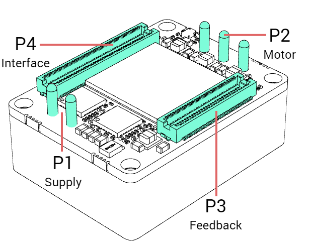
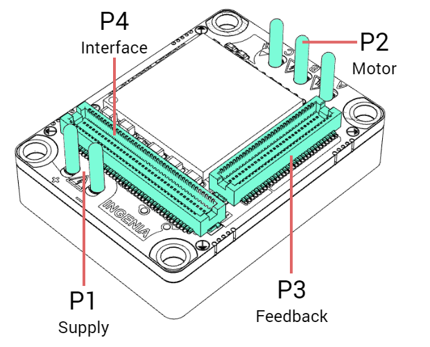
Everest NET connectors disposition Capitan CORE connectors disposition
While the mezzanine headers can only be connected to its matching mating connectors, the power pins can either be directly soldered to the interface PCB or be plugged into a receptacle mating contact. The first approach would allow Everest to reach its specified nominal phase current, but it will not be possible to unplug it from the interface board. On the other hand, the second approach will limit Everest to the rated current of the contacts, but enable it to be unplugged if required. In the case of Capitan, and provided the rating of the receptacle contacts is greater than the nominal current of Capitan, both strategies can be used while keeping its ratings intact. Therefore, the pluggable approach is highly recommended for Capitan.
Both strategies will require TH pads to hold the drive, meaning that a full footprint for EVE/CAP requires mixed assembly technologies, both THT and SMT.
Downloads
The following files are Altium Designer templates that are intended to facilitate and speed up the design. Although it is possible to start designing from scratch, Ingenia encourages designers to profit from the experience and knowledge embedded into the following contents.
| Product | Integrated Library | Device Sheet Module | Project Example |
|---|---|---|---|
Everest NET | |||
Everest CORE | |||
Capitan NET  | |||
Capitan CORE  |
These files include:
- Altium Integrated Library: contains the symbols and footprints for EVE/CAP as well as for the required PCB mating connectors, power pin contacts, and standoffs.
- Altium Device Sheet Module: allows to easily add EVE/CAP plus all the components required to plug it to an Altium project.
- Altium Project Example: simple Altium project template where the EVE/CAP module has already been added to schematic and PCB.
The EVE/CAP component
The EVE/CAP is not directly plugged into a PCB, but instead, it uses components to be plugged to, either along with the direct solder or the pluggable approach. These components are:
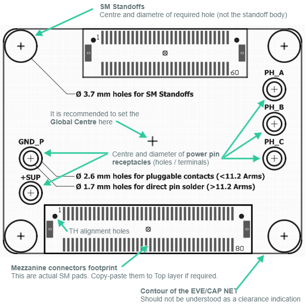
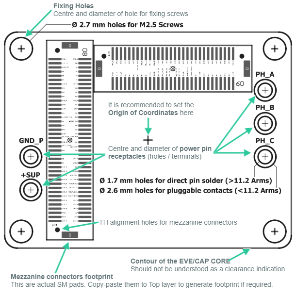
- Standoffs: / Fixing holes 3 mm board-to-board SMD standoffs are preferred in front of traditional standoffs, as once soldered they cannot move, thus making it easier to respect the small clearances to surrounding copper or components. EVE-CORE does not use them; instead, fixing holes for M2.5 screws are required to fix the aluminum chassis to the Interface board.
- Signal connectors: 60-pin and 80-pin mezzanine male mating connectors.
- Power pin receptacles: mating terminals (Mill-Max 9801-0-15-15-23-27-10-0, except EVE-CORE, which requires the pass-through variant Mill-Max 9372-0-15-15-23-27-10-0) for pluggable approach or TH holes for soldered approach. Both are disposed as independent components, yet the holes do not entail any BOM (only copper).
Plugged vs. Soldered approach
Pluggable approach would require terminals P1, P2, P3, P4 and P5, while soldered approach would require holes H1, H2, H3, H4 and H5. In the downloadable Device Sheet Module both sets of elements are superposed in the PCB (this will be shown as a component clearance conflict). Whichever is the selected approach, remove the components for the other from schematic, and then update the PCB. When only 1 of the 2 sets of components remain in the PCB, the conflict should be gone.
Notice this means that the EVE/CAP component does not have any terminals nor copper in its footprint. The copper comes from the mating and fixing elements listed above. However, the PCB component does include some critical information in various of its mechanical layers:
- Mechanical layer 5: can be used as a positioning guide for the required mating and fixing elements.
- Mechanical layer 10: contains the bounding boxes and designators for each component, used to generate the Assembly Drawing 2D output. If the EVE/CAP is flipped from Top to Bottom layer, this information should move to Mechanical layer 11, according to the defined layer pairs.
- Mechanical layer 13: contains the 3D body of the drive in a native STEP AP214 format (STEP file alone can be downloaded from the Dimensions section of each Product's Manual).
- Mechanical layer 15: contains critical information on clearances to nearby components, as well as routing considerations.
Mechanical layer 5: positioning guide
This layer contains useful mechanical data, including the centre of all the mating and fixing components, as well as their diameters or bounding boxes. It also includes a full footprint representation of the 2 mezzanine connectors, plus their proper orientation with first and last pins marked.
Footprint of mezzanine connectors
Mechanical 5 includes the footprint of the 2 required mating mezzanine connectors. It is not made out of rectangular shapes representing copper, but actual numbered SM and TH pads. Therefore, to generate a footprint for the mezzanine connectors, simply copy all the pads from Mechanical layer 5, and paste them into Top layer. Do not copy the text specifying the pinout, as it would be considered copper in the Top layer.
For Everest NET and Capitan NET:
For Everest CORE and Capitan CORE:
Then, to comfortably build-up the full EVE/CAP landmark, drag-and-drop each mating connector and fixing component with reference to their respective centres to the centre positions marked in Mechanical 5. Do this carefully, or otherwise deviations of the mating elements from their correct positions could induce an excessive mechanical stress to the EVE/CAP when plugged into the PCB.
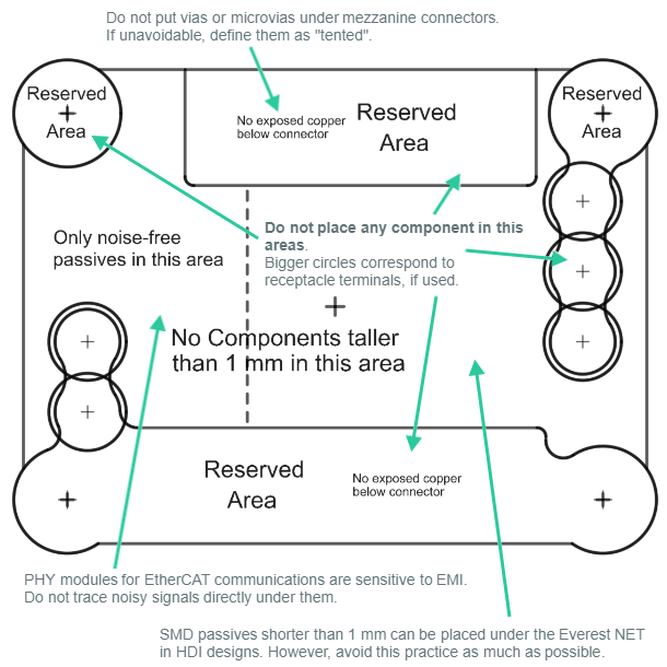
Mechanical layer 15: clearances
Considerations about clearances and general layout advice can be found in Mechanical layer 15. Understand the indications in this layer as the limits for component placement outside or below the drive.
For Everest NET and Capitan NET:
For Everest CORE:
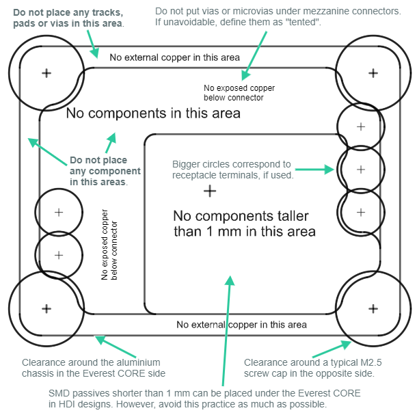
HDI designs with strong size constraints can benefit from placing components directly under the EVE/CAP, whenever they are under 1 mm height. However, this has to be done very carefully, not only with a total certainty on the height of the component and its tolerance, but also discarding any trace or component that could become both an "aggressor" or "victim" from the EMC point of view. This is specially important under the PHY modules, as the whole EtherCAT communications could be affected by a nearby radiating trace or a capacitive coupling.
As an example, do not trace the copper connected to the power pins towards the inside of the EVE/CAP, but towards the outside. This would prevent the power signals from affecting sensitive circuits of the drive.
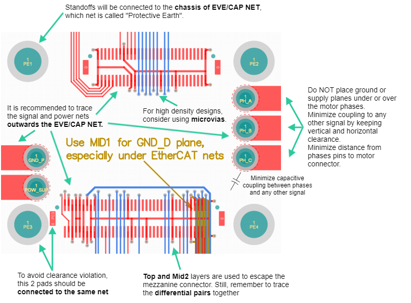
Layout considerations
The attached snippet includes the footprints of the mating and fixing components, as well as a basic layout proposal. Only signal traces are represented, with the purpose of pointing the most appropriate way of leaving the drive. As a rule of thumb, it is preferred to not direct the tracks towards the inside of the drive landmark, but outwards.
It is always strongly suggested to plan the physical distribution of components before start routing.
CRUCIAL LAYOUT RECOMMENDATION
The motor phases are the main source of EMI on most interface boards. The switching transients of the phases take few ns with harmonics at 100s of MHz and can get coupled to nearby signals and create several interference and EMI problems. Please:
- Minimize capacitive coupling from the phases to any other signal. Specially to sensitive signals such as analog, feedback or communications.
- Keep horizontal distance between phases and other signals or ground planes > 0.3 mm.
- Keep vertical distance between phases and any other signals > 1 mm.
- The distance between the drive phases to the motor connector should always be minimized whenever possible. Short tracks reduce losses and EMI.
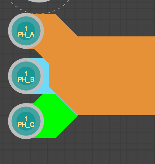
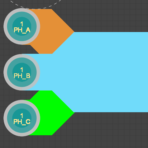
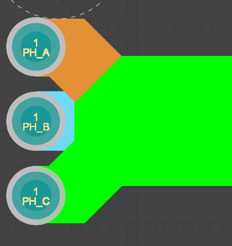
- It is OK to have couplings between the phases A, B, C. Indeed this minimizes common mode noise. The phases can be routed in parallel (OK) or coplanar on different internal layers (PREFERRED).
- Never pass signals between the phases as this could cause a strong magnetic coupling.
- When placing a series EMI filter on the motor phases such as a common mode choke or line inductor place it as close as possible to the drive.
- If the phases should be shielded on the PCB please:
- Shield them with GND_P or PE but NEVER shield them with GND_D or GND_A. This would make the logic grounds "dirty".
- Maximize horizontal and vertical distance from the phases to the shielding planes as indicated above. Shielding should act as a Faraday cage for the electromagnetic field but the capacitance to GND should be still be minimized to reduce conducted EMI.
Not following this considerations is the single most common mistake when designing interface boards and creates several problems that may require extensive filtering and traumatic workarounds. A good PCB layout can sometimes be better than several ferrites.
For Everest NET and Capitan NET:
For Everest-CORE:
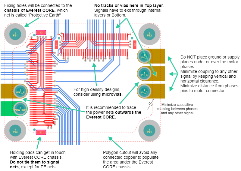
In the proposed layout, copper in Top layer is represented in red, Mid layer 1 is represented in yellow and Mid layer 2 in blue and the rest of layers in green (some tracks might be hidden in the image). This proposal also uses simple TH vias sized to fit a very attainable Class 6 PCB manufacturing category. This is a quite average level of sophistication, in terms of PCB manufacturing technology, but is sufficient to interface the EVE/CAP, thus entailing a cheaper cost. However, very dense designs might go for a less restrictive PCB Class, specially when most of the signals in the mezzanine connectors are used.
Use of vias or microvias
Although not specifically required, designs where most of the signal pins are used at the same time may consider interfacing the mezzanine connectors with microvias between Top and Mid 1 layers instead of classical TH vias. Note that this might entail higher PCB manufacturing costs.
GND_D below EtherCAT tracks in NET versions
It is highly recommended to reserve the whole Mid 1 layer to set a copper plane connected to GND_D; this is of an special importance in the area that is directly below and over the EtherCAT tracks going through Top and Mid 2 layers. This way, a low inductance return path is guaranteed to minimise any possible EMC issue.
But in the event there is no possible way to set this continuous GND_D plane along the EtherCAT tracks path, be sure to not overlap any of the 4 differential pairs along directly adjacent layers: this could cause a substantial cross-talk due to capacitive coupling, which can lead to serious malfunction of the communications. On the other hand, overlapping the positive and negative tracks of the same differential pair along directly adjacent layers is might be acceptable.
Area in contact with the chassis in EVE-CORE only
The chassis of Everest CORE will be in direct contact with the Interface PCB surface. As the thin layer of soldermask does not provide a sufficient isolation, it is mandatory to keep the contact area free of copper. No tracks, vias, pads or (obviously) components are allowed in the contact area, which means the signal tracks must exit the Everest Core along internal layers or Bottom layer. It is recommended to use Mid layer 2 for the signal tracks and keep mid layer 1 as a mostly uniform ground plane connected to GND_D.
The Mechanical 15 layer provided indicate the minimum recommended clearances around the contact area of the chassis.
Internal layers in Everest CORE snippet
Power tracks going through any layer from Mid 1 to Bottom are fine to exit the Everest CORE, but respecting the intended layer stack usage is advised (see below): GND_P will be better fitted through a layer dedicated to ground planes, as Mid 1, and POW_SUP will be better fitted in a layer dedicated to power supplies, as Mid 3 in this example. Motor phases, however, can go through any of these, but it is of special interest to not travel along an adjacent path to a ground plane, as this may cause an unwanted capacitive coupling between the motor phase and the voltage reference of sensitive circuits. This is why the motor phases are traced along Mid 1 in the given snippet.
Whenever possible, do not overlap power and signal (digital or analog). If some PCB areas are reserved for power tracks, all layers inside the area canshould be used for power tracks, maximizing copper area and reducing coupling to digital signals or digital ground (GND_D). In this situation, we suggest routing POW_SUP and GND_P in consecutive layers, increasing the capacitance between GND_P and POW_SUP. Same overlapping of signals can be done on PHASE power tracks.
Maximization of copper area
Overlapping motor phases between them is not a problem and minimizes its inductive coupling to other nets, reducing EMI noise. On the contrary, its coupling with GND_P or POW_SUP is far more dangerous from the EMI point of view.
For this reason, when multiple layers are used for routing power, instead of routing phases in parallel, it is recommended to use a different layer for each phase. This maximizes the copper surface used and minimizes coupling to other nets.
Proposed Layer Stack
Although many other options may be valid, here this 6-layer stack is proposed considering that is pretty standard, and targets the lowest PCB manufacturing cost to allow routing the drive comfortably. The resulting PCB should be around 1.6 mm thick.
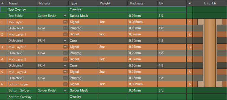
Note that internal layers are defined as 70 µm copper thickness. Specially when targeting the nominal phase current of Everest, this would help minimising the number of layers required to carry the phase currents without causing considerable losses due to self-heating. However, this might entail jumping from PCB Class 6 to Class 7 in some cases. Consult your PCB manufacturer. Also, in very small designs where the phases copper self-heating cannot be easily evacuated, consider selecting FR-4 dielectrics with higher glass transition temperatures: Tg = 150 ºC or even Tg = 180 ºC.
As for the example provided, the following usage of each layer is suggested:
| Layer | Usage in signal areas | Usage in power areas |
|---|---|---|
| Top | Components, signal tracks, GND_D | Components, tracks, GND_P |
| Mid 1 | GND_D copper plane | GND_P, PHASES |
| Mid 2 | Signal tracks, GND_D | POW_SUP, PHASES |
| Mid 3 | Power supplies | POW_SUP , PHASES |
| Mid 4 | Signal tracks, GND_D | GND_P, PHASES |
| Bottom | Components, signal tracks, GND_D | Components, tracks, GND_P |
If using µvias
For higher density designs using µvias from Top to Mid 1, it is recommended to switch the purpose of Mid 1 and Mid 2, tracing the signal tracks along Mid 1 and reserving Mid 2 to set a ground plane connected to GND_D.
Proposed Design Rules
Again, many options are plausible here, but consider this specific set of rules as the minimum required to integrate the EVE/CAP without entailing an additional handicap.
| Rule | Value |
|---|---|
| Minimum clearance to Power conductors (external layers) | 0.5 mm |
| Minimum clearance to Protective Earth (chassis) | 0.5 mm |
| Minimum distance between Signal conductors (internal & external layers) | 0.15 mm |
| Minimum track width (internal & external layers) | 0.15 mm |
| Minimum component body clearance | 0.2 mm |
| Minimum annular ring (internal & external layers) | 0.15 mm |
Minimum plated hole diameter | 0.2 mm |
| Hole to hole clearance | 0.3 mm |
| Paste mask expansion | 0 mm |
| Solder mask expansion | 0.05 mm |
| Minimum solder mask sliver | 0.07 mm |