Product Description
The Titan Go Servo Drive is a high power density solution providing top performance, advanced networking and built-in hardware and firmware based safety, as well as a fully-featured motion controller. It can control multiple motor types and supports almost any feedback sensor including absolute serial encoders and resolvers.
Its design includes multiple communication ports as CANopen, RS-485, USB all of them are electrically isolated.
The Titan Go Servo Drive has been designed with efficiency in mind. It incorporates cutting-edge power semiconductor technology as well as optimized control algorithms to provide the perfect trade-off between electromagnetic emissions and performance.
Titan part numbering
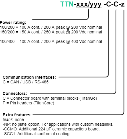
| Ordering part number | Status | Image |
|---|---|---|
| TTN-150/200-C-C-CCMO | PRODUCTION | - |
| TTN-100/400 | OBSOLETE | - |
Specifications
A list of features of the Titan Go Servo Drive is shown next.
Electrical and power specifications | ||
|---|---|---|
| Part number → | TTN-150/200 | TTN-100/400 |
Power supply voltage | 10 VDC to 200 VDC | 10 VDC to 400 VDC |
| Auxiliary logic supply input voltage range | 10 VDC to 65 VDC | |
| Standby logic supply consumption | ≤ 10 W | |
| Transient peak voltage | 220 VDC | 450 VDC |
| DC bus capacitance | 63 µF (+224 µF if CCMO version is chosen) | |
| Minimum motor inductance | 50 µH (for low inductance motors use high PWM frequency mode) | 50 µH |
Nominal phase continuous | 150 ARMS (with heatsink) | 65 ARMS (with heatsink) |
Nominal phase continuous | 150 ADC | 65 ADC |
Maximum phase peak current | 250 ADC (1 s) | 85 ADC (1 s) |
| Current sense range | ± 457 A (Versions 1.0.0 and 1.1.0) ± 359 A (Version 1.2.0) | |
| Current sense resolution | 893 mA/count (Versions 1.0.0 and 1.1.0) | |
| 701.8 mA/count (Version 1.2.0) | ||
| Shunt braking transistor | Low side shunt braking transistor on board. 100 A continuous braking current capacity. | |
| Inrush current | < 10 A at connection. Titan includes a 2 kΩ DC bus capacitor precharge resistor that limits the inrush. No need for external capacitor precharge circuits or relays. | |
| Cold plate | 7 mm aluminum plate 6082-T6. | |
| Power connectors | Power ring terminals with M8 screws and washers included. The maximum absolute screw torque is 9 Nm. Do not exceed 9 Nm in any axis to the power connectors, take care of bus bars and thick motor cables. | |
Efficiency | >97% at the rated power and current. Note that the 400 V 100 A version is more efficient at low load, while the 200 A version is efficient at high load. | |
Motion control specifications | ||
Supported motor types |
| |
Power stage PWM frequency | 10 kHz (default) | |
| Current sensing | Isolated current sense on phases A, B, and C. | |
Sensors for commutation (brushless motors) |
It is recommended to install the SSI only firmware variant if absolute encoder SSI is used for commutation. | |
| Sensors for servo loops |
| |
Supported target sources |
| |
| Resolver specifications |
| |
Inputs/outputs and protections | ||
| General purpose Inputs and outputs |
| |
| Dedicated Inputs and outputs |
| |
| Output Supplies |
| |
Protections |
| |
| Safe Torque Off | 2 x STO inputs, 24 V isolated inputs (work from 15 V to 30 V). Redundant topology with self-test features. Ready for SIL 3 reliability level but not certified. 1 x STO feedback indication output for external self-verification circuit. Minimum pulse width for Safe Torque Off activation (and power stage shutdown): 14 ms Minimum pulse width for STO feedback reaction: 1 ms. Pulses < 1 ms can be used for safety PLCs but will be ignored. Pulses between 14 ms and 1 ms can be used for self test. | |
| Motor Brake | Not available. | |
Communications | ||
| USB | MiniUSB (2.0) vertical connector. Fully isolated 2.5 kVRMS 1 min. | |
| Serial | RS-485 full-duplex (compatible with RS-422) isolated 2.5 kVRMS. Default 115200 bps, 8 data bits, no parity, 1 stop bit, no flux control. 120 Ω terminations for TX and RX included on board with DIP switches. TX+ and RX+ biased to +5 V with 4.7 kΩ. TX- and RX- biased to GND with 4.7 kΩ. | |
| CANopen | CANopen compliant with isolation (self powered, no need for external supply). 1 Mbps max (default). 120 Ω termination included on board with a DIP switch. CiA-301, CiA-303, CiA-305, CiA-306 and CiA-402 compliant. | |
| EtherCAT | - | |
Environmental and mechanical specifications | ||
Part number → | ||
| Cold plate temperature |
| |
| Heat dissipation | The maximum heat dissipation is 4 kW. Provide a heatsink according to environment temperature and power rating. Heat dissipation is affected mainly by the phase current and voltage. In order to achieve the maximum power ratings, excellent heat transfer is needed between the cold plate and a heatsink. Please see Dimensions and assembly for details. | |
| Maximum humidity | 5% - 85% (non-condensing). Titan can be supplied with conformal coating. | |
| Horizontal dimensions | 206 x 172 mm | |
| Maximum height | 55 mm | |
| Weight (exc. mating connectors) | 1878 grams | |
Hardware revisions
Hardware revision | Individual board references | Description and changes |
|---|---|---|
1.0.0 May 2017 | i047-01H1-1.0.0 i047-01H2-1.0.0 i047-01H3-1.0.0 | First product beta release. |
1.1.0 September 2017 | i047-01H1-1.1.0 i047-01H2-1.1.0 i047-01H3-1.1.0 | First product release. Changes from the previous version:
|
1.2.0 January 2018 | i047-01H1-1.2.0 i047-01H2-1.2.0 i047-01H3-1.2.0 | Improvements in current sensing and EMI at high current performance.
|
Identifying the hardware revision
Hardware revision is screen printed on the board. It can also be read from Motion Lab - Drive parameters.
Power and current ratings
TTN-x/xx-C-C variants of Titan Go are capable of providing the nominal current from -40 ºC to 85 ºC (temperature measured in the cold plate) with a 0.1 ºC/W heatsink (Fischer LA 11 200 24) attached by means of a low thermal resistance interface material. Above 85 ºC a current derating could be needed to prevent overheating. Above 85 ºC a current derating could be needed to prevent overheating. Please see Dimensions and assembly for further details.
In case of excessive power losses, over-temperature will be detected, causing the driver to turn off. The system temperature is available in E-Core registers and is measured near the power stage. This temperature parameter can be accessed from USB 2.0, CAN or RS485 serial interface and does not indicate the air temperature, but the temperature of the PCB. Above 110 ºC the Titan Go automatically turns off the power stage and stays in fault state avoiding any damage to the drive. The Fault LED will be activated and latched until the temperature decreases below this threshold.
Drive safety is always ensured by its protections. However, by means of it, power losses and temperature will limit the allowable motor current.
Some parts of the Titan Go can exceed 125 ºC during operation, especially at high load levels.
Do not touch the Titan Go during operation and wait at least 5 minutes after turn off to allow a safe cool down.
The following figure shows the basic power flow and losses in a servo drive system.
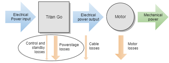
Power losses calculation (heat dissipation)
Current flowing through Titan Servo Drive causes power losses that, ultimately, are converted in heat. This heat must be transferred to its surrounding environment efficiently so that the temperature of the drive does not reach dangerous levels. The greater the power losses, the more effective the heat dissipation must be. Power losses mainly depend mainly on 3 parameters:
- Motor RMS current: this is the cause of what is called static or conduction power losses, which typically are the main source of power losses, having that they show a positive correlation in a squared ratio.
- DC bus voltage: this, along with the motor RMS current and PWM switching frequency, is the cause of what are called dynamic or commutation losses, and show positive correlation in a proportional ratio.
- PWM switching frequency: similar to DC bus voltage, the PWM switching frequency directly affects the commutation losses. Typically, 10 kHz is the default value to reduce these losses, but it can be increased up to 20 kHz.
PWM switching frequency and nominal specifications
All nominal specifications in this manual are measured under a PWM switching frequency of 10 kHz.
PWM in SMO feedback mode
It is strongly recommended to configure the alternative PWM frequency of 20 kHz when using the sensorless SMO as a feedback source, or when controlling motors of low inductance.
Other less relevant parameters affect also the power losses but are not considered in the following graphs:
- Air temperature: higher power semiconductor temperatures reduce their efficiency.
Motor speed: faster motor speeds result in higher overall power losses since the input DC bus current is greater, and this increases conduction losses on the reverse polarity protection circuitry.

Current ratings
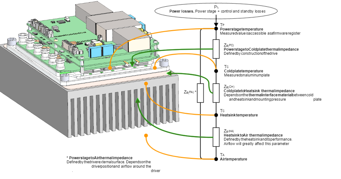
Power losses cause the drive to increase its temperature according to:
As power losses have a positive correlation with the motor RMS current, when the ambient temperature rises, the output current must be limited to avoid an excessive drive temperature (TP < 110 ºC). The threshold temperature where the current derating should start mainly depends on the DC bus voltage.
| Parameter | Value | Units | Notes |
|---|---|---|---|
| Maximum absolute power stage temperature | 110 | ºC | Measured on the PCB (not the heatsink) and accessible via register. |
| Thermal resistance from power stage to the heatsink | 0.017 | ºC/W | Does not consider the thermal resistance of the heatsink, but assumes the cold plate is a thermal conductor, not the thermal dissipator. |
| Thermal resistance from power stage to air | 5 | ºC/W | Considering the drive is vertical and free air convection with is allowed on the cold plate surface (> 30 cm clearance around the drive). Mounting the drive without heatsink could only be done for very low load applications or debugging purposes, otherwise, over-temperature alarm will occur after a few minutes of operation. |
| Temperature stabilization time | 800 | s | With 0.1 ºC/W heatsink attached. Considering 90 % of the maximum temperature. |
This graphic shows the maximum current with respect to ambient temperature, also assuming a 0.1 ºC/W heatsink attached.

Current derating
The current derating graph is only indicative and is based on thermal tests performed in a climatic chamber where there was enough room for natural air convection. Each application may reach different ratings depending on the installation, ventilation and/or housing.
Current derating is only a recommendation and is not performed automatically by the drive.
Maximizing heat dissipation with a heatsink
A heatsink is needed to reach the nominal current at any ambient temperatures. When using high-efficiency heatsinks or in enclosed spaces, the equation can be simplified as follows.
Assembly recommendations for best heat dissipation
- Always allow natural air convection by ensuring ≥ 10 mm air space around the drive.
- Use a good thermal interface material to improve the heat dissipation. See Dimensions and assembly for details.
- If housed, use a good thermal conductivity material, such as black anodized aluminum. Placing the drive in a small plastic package will definitively reduce its temperature range.
- Temperature range can be increased by providing forced cooling with a fan. Always ensure electrical isolation between live parts and the heatsink.
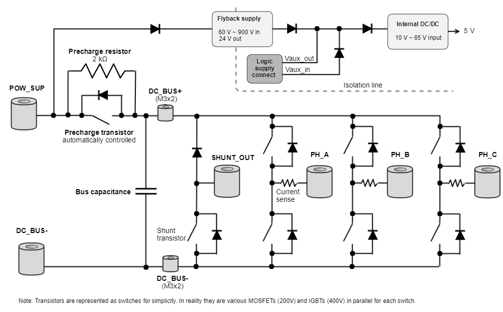
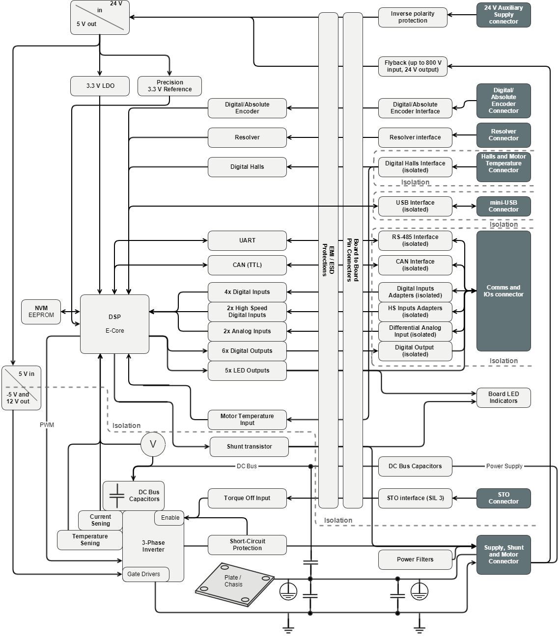
Architecture
This diagram represents the main hardware elements of Titan Go, and how they relate to each other.
Power stage and supply architecture
The following drawing shows the architecture of the power stage and its main components. Also, it clarifies how the internal power supplies are wired. For simplicity, power transistors are shown as switches.