Schematic Design
Everest and Capitan are designed to be interfaced at 3.3 V levels (or otherwise specified). However, when interfacing other devices, such as sensors, command sources or master controllers, additional adaptor electronics might be required to cover a wider range of input voltages. Here, some circuits are suggested as a reference design for a quick-development of an interface board.
About this solution
Notice this solutions are designed to be simple, cost effective, and easy to manufacture. Other solutions from those presented here may also be valid, and even be more suitable, depending on the approach or design constraints.
Product Manual required
The information presented here is by no means a valid description of the capabilities of each product, but a set of suggestions only. Therefore, it is advised to use this guide together with each drive's specific Product Manual. Particularly, see the Product Description (EVE-NET, EVE-CORE, CAP-NET, CAP-CORE) and Pinout (EVE-NET, EVE-CORE, CAP-NET, CAP-CORE) sections for the most crucial information on the limits and capabilities of each drive.
Wiring information
The contents of this Application Guide are limited to the circuits contained in an hypothetical interface board to hold the EVE/CAP. However, how this interface board should be wired to the actual motor, supplies and sensors in the end-user application environment is a topic of major relevance. In this regard, it is suggested to take a look at the Wiring and Connections chapter of the Everest XCR and Capitan XCR Product Manuals, which focuses on the proper wiring practices of Ingenia's approach of an EVE/CAP NET interface board.


Ingenia recommends to only select RoHS compliant components for designing products which life cycle can easily adhere to WEEE directive.
Input Supplies
DC Power Supply
Although typically not part of the interface board, but wired outside, this could be one of the main and first elements to take care of, as the way it is dimensioned could affect the rest of the design. The drive generates 3-phase currents by means of an inverter topology power stage, so it require a DC power supply to feed its internal DC bus. Selecting the proper voltage, current and power of this supply is typically not as simple as checking the specifications of the target motor. In fact, in most cases the nominal values of the motor will be substantially different from the analogous values of the power supply. To learn more about this, check out the following documents:
DC Bus Input Stage
EVE/CAP is a switched power regulator using a very fast switching technology. This allows EVE/CAP to be very efficient, but at the cost of requiring a relatively more sophisticated input stage to avoid transmitting a "sharp" ripple voltage through the power supply lines. This is of an special importance when sharing the DC bus with other sub-systems or when targeting EMC-related certifications, such as CE marking. The most suitable solution will strongly depend on the requirements of:
- The target market or environment (industrial, medical, domestic, automotive...) and the EMC standards that apply to each application.
- The construction of the motor, specially its inter-winding capacitance and winding-to-chassis capacitance. The lower these capacitances are, the better.
- The distance between the drive and the motor (length of the phase wires), with the best case being the drive mounted inside the motor metallic housing, which also acts as a "Faraday cage".
- The voltage and current of the application.
Depending on these parameters the filter can be chosen and tuned, but either way it will typically consist on the following elements:
- Input power filter
- Earth decoupling
- DC bus bulk capacitors
- Sourge / ESD protections
The 2 first elements can be resolved by means of a line filter. A 1-stage line filter might be enough in some cases, but in most cases a 2-stage filter would make it to pass the conducted emissions tests. Anyhow, a line filter might be very bulky compared to the drive, so the on-board discrete solution can be the best trade-off. Here, only very basic and raw indications are given:
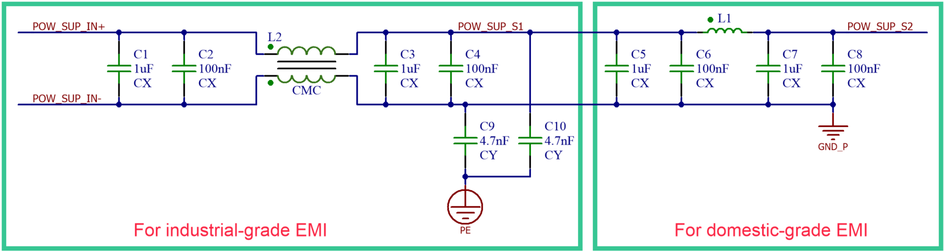
The basic protection to fulfil the minimum requirements of most industrial-grade EMC certifications would consist in a power filter targeting the common mode of the DC bus. The input and output capacitors are separated into 1-decade pairs to extend their effectiveness to higher frequencies (this could be done up to 2 decades or even more). The selected values just pretend to be indicative of this. This capacitors should be of X-type ceramic and their voltage must be carefully selected to match the application under a "safety" criteria: keep in mind that capacity of ceramic capacitors experience a strong derating over voltage. Decoupling capacitors to Earth C9 and C10 are of crucial importance. They must be of Y-type and rated to safety standards, specially when it comes to have its failure mode guaranteed.
For more demanding EMC requirements, like certifications framed in domestic or automotive standards, an additional filter targeting the differential mode might be required. Here a C-L-C or Pi filter is suggested, although many others may be valid. This filter is intended to reduce the voltage ripple in the DC bus caused by the fast commutation of the Drive, as it propagates through the cables affecting both the conduced and radiated frequency ranges. This is strongly related to the load, as inductance and current ratings of the motor directly affect the DC bus voltage ripple, but DC bus bulk capacity plays a notable role in reducing this effect (see below). In any case, selecting an L1 small enough might be demanding, specially when sized to withstand the current ratings of the drive.
Suggested values for inductor L1 may range between 100 nH and 100 µH depending on the conducted EMC requirements. It is typically preferred to increase the DC bus capacitance on the driver side instead of including larger inductance.
Regarding the Common Mode Choke (CMC) L2, a common mode inductance ≥ 1 mH could be a good starting point. Contact Ingenia for further help on this topic.
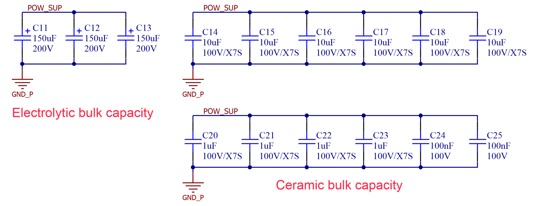
Second, the DC bus bulk capacity plays a crucial role in the EMI response, but also in the motion control by reducing DC bus ripple. As a dummy rule of thumb, the greater the installed capacity, the better, but at the same time capacitors are big and expensive, so optimising the number and type of the capacitors included in the design is usually something to take care of. Typically, having these capacitors will respond to 3 purposes:
- Reduce voltage ripple in the DC bus to improve conducted EMI.
- Reduce voltage ripple in the DC bus to reduce the capacitor's self power losses or the power loss throughout the supply wires.
- Store excess of energy during regenerative braking.
The solution suggested here does not rely on the DC Bus capacitors to narrow down the regenerative braking issue, provided an specific circuit is proposed to this purpose below in this guide (see the Shunt Braking Resistor Transistor chapter). Then, when it comes to reduce the DC bus voltage ripple, it is interesting to distinguish between 2 phenomena shaping it. In the image below this 2 types of ripple are depicted. The top one has more amplitude, but edges are round and soft, so it mostly carries lower frequency harmonic components. The bottom one has less amplitude, but has sharp edges of a great dV/dt, so it carries higher frequency harmonics. Typically the DC Bus voltage will be affected by this 2 types of ripple at the same, but the magnitude of each will typically depend on the amount of current delivered to the motor, and its phase inductance.
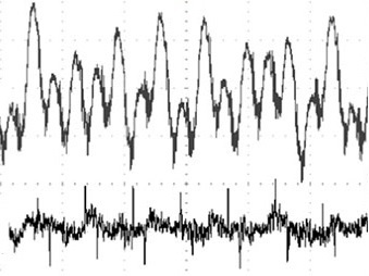
High frequency ripple is more likely to increase when the drive is delivering high phase currents. This ripple does not carry much overall energy, but requires capacitors capable of responding to high frequencies with low ESR. Therefore, the best option here are ceramic capacitors, which nowadays typically outperform other capacitor technologies, like tantalum, electrolytic or polymer. Although the minimum required ceramic capacity is already included inside the EVE/CAP, it is strongly suggested to add at least 30 µF X7R/X7S ceramic capacity externally as close as possible to the power supply terminals of the drive, to get a reasonable performance in a mid-range application.
Low frequency ripple is more likely to increase when the EVE/CAP is driving a low inductance motor, specially when driving it at high currents. This ripple can get to carry a lot of energy, and therefore a larger capacity would be required. Here, ceramic capacitors are still the best choice, but installing a large bank of ceramic capacity can be space-consuming and very expensive, while electrolytic capacitors, specially aluminium electrolytic capacitors, show much better ratios in capacity per volume at a lower cost. However, be aware that having electrolytic capacitors in a commercial product might entail serious drawbacks: they can contain dangerous chemicals, they can explode if mounted in reverse polarity, they could limit the temperature rating of the whole product, and they would probably become the shortest lifetime component of the design (MTBF bottleneck).
Electrolytic capacitors
Ingenia recommends not to use electrolytic capacitors unless there is no other way to satisfy the requirements of an application. In such case, select only the highest quality capacitors, with specs such as:
- Temperature rating > 100 ºC
- Low ESR / high ripple withstanding
- Certified lifetime at high temperature (MTBF) > 6000 hours.
Also, always apply a over-dimension in the voltage rating of electrolytic capacitors of at least x1.3
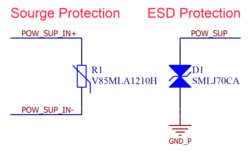
Finally, it is advisable to include surge and ESD protection in the power DC input to reinforce the immunity ratings of the drive. A TVS could do the job for ESD protection, but might be insufficient in front of a surge, where suppression of large but very short power peaks is not as relevant as the response in front of a wide and long high-energy peak. To this purpose, varistors are more suitable. As a useful tip, in case a discrete line filter is implemented, it is recommended to place the TVS after the common mode choke: as a CMC acts like an impedance barrier (from the signals propagation point of view) perturbations in the internal DC bus could become fast and short overvoltages when reflected in the CMC. If any of this reflections reaches a dangerous level, the TVS would get rid of it.
With all this, the following generic solution is proposed:
Schematic
Ceramic and (optional) electrolytic capacitors:
Surge and ESD protection:
Signals description
Signal | Description |
|---|---|
| POW_SUP_IN+ | Positive terminal of the power supply input |
| POW_SUP_IN- | Negative or reference voltage terminal of the power supply input |
| POW_SUP | Internal DC bus positive supply. Could be connected to the EVE/CAP power pin 1 of P1 if no inverse polarity protection is implemented |
| PE | Protective Earth. To be connected to the chassis of the EVE/CAP. Could be left unconnected in specific cases |
| GND_P | Internal DC bus reference voltage. To be connected to power pin 2 of P1 in EVE/CAP |
Design Notes
- POW_SUP net would be connected to POW_SUP_S1 or POW_SUP_S2 depending on the line filter implemented. If no line filter is on-board, it would be connected to POW_SUP_IN+.
- Select a bidirectional TVS if an inverse polarity protection is implemented (see below), and unidirectional TVS otherwise.
- Electrolytic capacity would not be required in most cases.
- Ceramic capacitors should be placed as close to the drive as possible, keeping the smallest in capacity as the closest to P1 pins.
Maximum DC bus supply voltage rating
The selected TVS is rated 70 V standoff voltage instead of 80 V. About 1 mA will be sunk through it while the DC bus is supplied to 80 V, but this should not entail a great power loss. On the other hand, by doing this the lower maximum clamping voltage will result in a more effective protection for EVE/CAP.
Bill of materials
Designator | Part Number | Manufacturer | Package | Value / Description |
|---|---|---|---|---|
| C9, C10 | GA355DR7GF472KW01L | Murata | 2220 | X1/Y2 safety capacitor 4.7 nF -40ºC ~125ºC |
| L2 | CM5441Z101B-10 | Laird | 4 pin Through Hole | 2 Line Common Mode Choke Through Hole 100 Ohms @ 100MHz 75A DCR 0.3mOhm |
| L1 | ETQ-P5MR68YLC | Panasonic | SMD 10x10mm | Fixed Inductor 680nH 31.5A 1.93mΩ |
| C11, C12, C13 | EKXG201ELL151ML25S | United Chemi-Con | Radial, Ø16x25 mm | Aluminium electrolytic capacitor, 150 µF, 200 V, -40 ºC ~105 ºC, MTBF 1000h @ 105 ºC, 1.89 A @ 100 kHz current ripple |
| C14, C15, C16, C17, C18, C19 | C5750X7S2A106K230KB | TDK | 2220 | Ceramic capacitor, 10 µF, 100 V, X7S |
| C1, C3, C5, C7, C20, C21, C22, C23 | C2012X7S2A105K125AE | TDK | 0805 | Ceramic capacitor, 1 µF, 100 V, X7S |
| C2, C4, C6, C8, C24, C25 | HMK212B7104KG-T | TDK | 0805 | Ceramic capacitor, 100 nF, 100 V, X7R |
| D1 | SMLJ70CA | Bourns | SMC / DO-214-AB | Bidirectional diode TVS, 70 V standoff, 113 V max. clamping, 3000 W |
| R1 | V85MLA1210H | LittlelFuse | 1210 | Varistor, 85 V DC standoff, 250 A max. surge current, 2.5 J max. surge energy |
Logic supply
EVE/CAP requires a 5 V regulated (better than 2%) supply is provided. There are several ways to generate the 5 V, and the best suited will probably be the one fitting the available power source from which to pick the logic supply, whether it is AC or DC. In most cases, the power supply to feed the DC bus will also be the source for the logic supply. In this case a DC/DC will be selected by matching its input voltage range to the maximum expected voltage of the DC bus (including any possible re-injection). This DC/DC could be typically implemented according to 3 approaches:
- A discrete DC/DC on board
- An integrated module mounted into the PCB
- A completely external DC/DC wired to the Interface Board.
All solutions are valid, providing the following specs are met:
- Input voltage: set by application (100 V will cover typical scenarios)
- Output voltage: +5 V
- Output voltage regulation: ±2% or less
- Output voltage rise time: between 2 ms and 10 ms
- Max. ripple: 200 mVp-p or less
- Output current: 700 mA continuous, 1 A continuous preferred.
- Isolation voltage: >1.5 kV recommended to prevent ground loops between digital and power, although not mandatory in some cases.
Ingenia is committed to a more efficient use of energy and recommends to always select the highest efficiency components.
Output current required
The minimum output current specified above is only for EVE/CAP, so does not include the Interface Board self-consumption or its capability to deliver current to other external circuits.
Initialisation sequence
To guarantee all the internal supplies fulfil an adequate power-up sequence, the 5 V supply must reach its nominal voltage in no less than 2 ms and no more than 10 ms. Otherwise, initialisation problems could appear, specially at the lowest or highest temperatures.
A couple o valid DC/DC examples:
Image | Part Number | Manufacturer | Type | Description |
|---|---|---|---|---|
 | RSD-30H-5 | Mean Well | External | 40 V to 160 V input, single 5 V output, 30 W, 4 kV isolation DC/DC |
 | SPBW06G-05 | Mean Well | PCB | 18 V to 75 V input, single 5 V output, 6 W, 1.5 kW isolation DC/DC |
Schematic
First, the proposed input stage has a TVS for ESD protection and an input filter. CLC might be good, but here ferrites are used instead instead of inductors for space saving and to focus the attenuation in the highest frequencies.
Second, 5 V is converted to 3.3 V by means of a simple LDO. The EVE/CAP does not consume any current from this 3.3 V, so it must be enough to cover the self-consumption of the Interface Board plus the amount of current to be sent to external circuits (see 3.3 V and 5 V Output Supplies chapter below). When the total power consumption of the interface board at 3.3V is less than 250 mA, this circuit is not necessary and the power can be obtained from pin 14 of connector P4.
Signals description
Signal | Description |
|---|---|
| +5V_IN | Positive terminal of the 5 V logic supply input |
| 0V_IN | Negative terminal of the 5 V logic supply input |
| +5V_D | +5 V Logic supply to feed both EVE/CAP and the Interface Board. To be connected to pins 7, 8, 9 and 10 (NET) or pins 3, 4, 5 and 6 (CORE) of EVE/CAP Interface connector |
| +3.3V_D | +3.3 V Logic supply to feed the Interface Board (if > 250 mA are needed on the interface board). |
| GND_D | Logic supply reference voltage. To be connected to pins 5, 6, 11 and 12 (NET) or pins 1, 2, 7 and 8 (CORE) of EVE/CAP Interface connector |
Design Notes
- D1 is a unidirectional TVS, meaning that in case of inverse polarity of the 5 V input this will conduce in direct mode. Then, either the power supply voltage will drop once reached the maximum current or the TVS will burn if the power supply is powerful enough. This behaviour is intended, as it works as a very basic inverse polarity protection in addition to its main ESD protection function.
- +5V_D must be connected to the 4 dedicated pins of EVE/CAP Interface connector. All 4 pins must be connected to reach a sufficient current rating from the contacts of the EVE/CAP Interface connector. Similarly, the closer 4 pins should all be connected to GND_D.
3.3 V pins from EVE/CAP
Pin 14 (NET) or 9 and 10 (CORE) of EVE/CAP is not an input supply input but a 3.3V output, therefore this pins must not be connected to a supply. EVE/CAP is providing this 3.3 V supply outputs to avoid adding external electronics when only simple external circuits are required. However, the maximum current to be drawn from this output is limited to 250 mA, and exceeding it might cause permanent damage to EVE/CAP, so it is not used in this application example.
Bill of materials
Designator | Part Number | Manufacturer | Package | Value / Description |
|---|---|---|---|---|
| C1, C2, C6 | GRM155R71C104KA88D | Murata | 0402 | Ceramic capacitor, 100 nF, 16 V, X7R |
| C3, C4, C5 | C2012X7S1C106M125AC | TDK | 0805 | Ceramic capacitor, 10 µF, 16 V, X7S |
| D1 | PTVS5V0S1UR,115 | NXP | SOD-123W | Unidirectional diode TVS, 5 V standoff, 9.2 V max. clamping, 400 W |
| L1, L2 | BLM18SG221TN1D | Murata | 0603 | 2.5 A ferrite bead, 220 Ω @ 100 MHz, 40 mΩ @ DC |
| U1 | LD1117S33CTR | ST Microelectronics | SOT-223-4N | 15 V max. input LDO, fixed 3.3V output, 800 mA |
Digital and Analog grounds disambiguation
EVE/CAP has different reference nets for the digital ground (GND_D) and analog ground (GND_A).
Use GND_D as reference for all digital circuits.
Use the GND_A as the reference ground for your analog circuits.
GND_D and GND_A connection
Nets GND_D and GND_A are internally connected using a ferrite bead.
- If analog signals are not used, do not connect GND_A on your board.
- If analog signals are used, do not connect GND_D and GND_A directly. Use a ferrite bead or 1 Ω resistor in between.
Protective circuits
Inverse Polarity Protection
This circuit is intended to block any current going into EVE/CAP when the power supply is connected in inverted polarity. If this circuit is not present, it is suggested to select a polarised power supply connector.
Effects of inverted polarity
Connecting the power supply under inverted polarity with no protection could cause permanent damage to EVE/CAP.
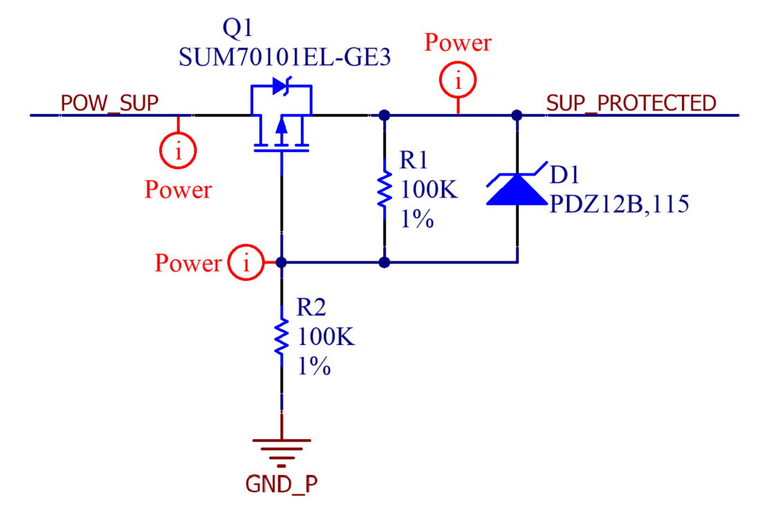
Schematic
Signals description
Signal | Description |
|---|---|
| POW_SUP | Input from power supply |
| SUP_PROTECTED | Protected power supply. To be connected to power pin 1 of P1 in EVE/CAP |
| GND_P | Power supply reference voltage. To be connected to power pin 2 of P1 in EVE/CAP |
Design Notes
- In this circuit, the P-channel MOSFET is only polarised properly when the polarity of the supply is correct thanks to resistors R1 and R2. Diode D1 ensures that the maximum gate voltage of the transistor is not exceeded.
- Note that the transistor orientation intentionally allows conduction through the body diode if the supply is polarised properly.
Bill of materials
Designator | Part Number | Manufacturer | Package | Value / Description |
|---|---|---|---|---|
| D1 | PDZ12B,115 | NXP | SOD-323 | Diode Zener 12 V, 400 mW, 2% tolerance |
| Q1 | SUM70101EL-GE3 | Vishay | TO-263 / D2PAK | P-channel MOSFET, 100 V, 120 A |
| R1, R2 | RMCF0402FT100K | Stackpole | 0402 | Thick film resistor, 100 kΩ, 1 % tolerance, 1/16 W |
Shunt Braking Resistor Transistor
During operation the motor normally consumes the energy provided by the drive, but in specific situations this roles change and the motor behaves as a generator. This would happen during short periods of time when the motor is commanded to rapidly decelerate or even change its direction of rotation, or during longer periods of time when the load is driving the motor, like it would happen when a hoist is overloaded. In this cases, although an inverter typically works as a "step-down", it will behave as a "step-up", and could elevate the voltage of the internal DC bus even beyond its maximum ratings, causing permanent damage to the drive and leaving the load completely uncontrolled.
Therefore, this is an over-voltage protection.
To get rid of the problem, 4 strategies are considered. The best one to follow would mostly depend on the dynamics of the load, so there is not a best solution to frame all the possible scenarios.
- Not doing anything: re-injection could not be an issue, specially when the nominal voltage of the motor is way smaller than the one of the drive (i.e. driving a 24 V motor with EVE/CAP). If the re-injection is not too strong, the internal DC bus of the drive will increase, but not enough to reach dangerous levels, so the drive will simply withstand it.
- Using the DC bus capacitors: if a large bulk capacity is installed close to the EVE/CAP (not long wires between them) when the DC bus voltage increases because of a re-injection, the capacitors will store the energy, and slowly deliver it afterwards to the motor during normal operation. This method is tremendously ineffective compared to dissipating the excess of energy, but it could do the job in front of short and fast re-injections that would not happen very often, like when the motor sporadically has to change direction of rotation .
- The system is battery powered: in this specific case, the re-injection charges the battery. In some applications, like electric vehicles, this might even be an advantage, as it would extend the battery life. However, care must be taken in ensuring that the re-injected current measured in the battery terminals is not beyond its maximum charging ratings. Also, when the battery is fully charged this method cannot be used.
- Get rid of the excess of energy: Here a transistor is used to short the DC bus to Ground through a power resistor, which would dissipate the excess of energy as heat. This method has proved to be the most effective (and the less efficient) but has the drawback of requiring a very bulky resistor, which is costly and space-consuming. This method can be implemented with the circuit proposed below.
To learn more about motor re-injection and how to dimension the power resistor, check the following document:
Multi-axis systems
Notice that in multi-axis systems or even when multiple drives share a same DC bus only 1 braking resistor is needed. Even some advanced power supplies have a braking resistor already integrated.
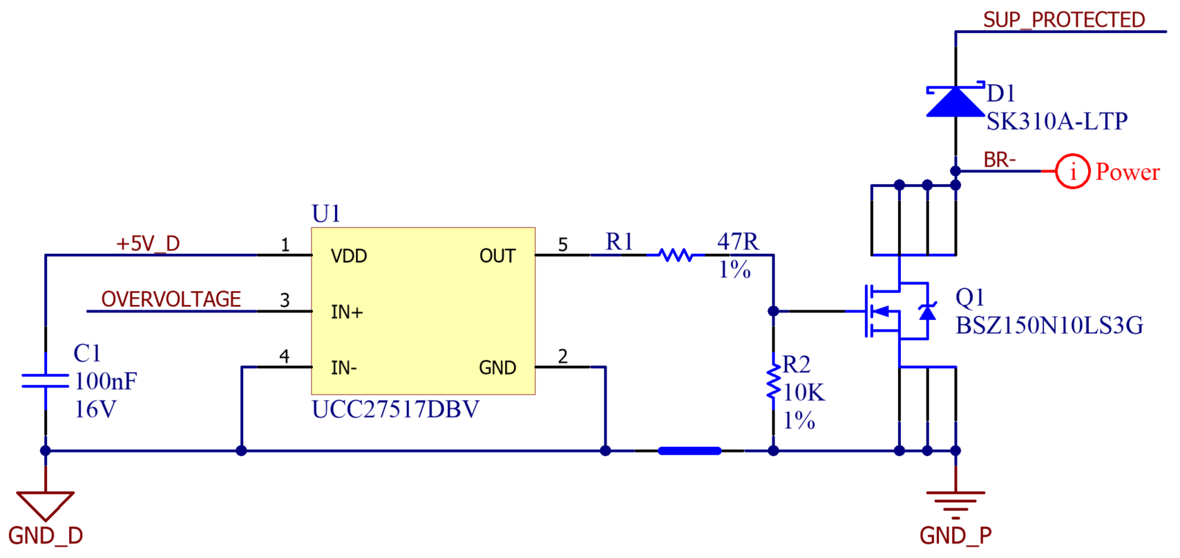
Schematic
Signals description
Signal | Description |
|---|---|
| +5V_D | +5 V Logic supply |
| OVERVOLTAGE | To be connected to any of the GPOx pins of EVE/CAP Interface connector |
| SUP_PROTECTED | To be connected to power pin 1 of P1 in EVE/CAP |
| BR- | To be connected to the negative terminal of the power resistor |
| GND_P | Power supply reference voltage. To be connected to power pin 2 of P1 in EVE/CAP |
| GND_D | Logic supply reference voltage. To be connected to pins 15, 16 or 35 of EVE/CAP Interface connector |
Design Notes
- OVERVOLTAGE net must be tied to any of the GPOx pins of EVE/CAP Interface connector (pins 17, 29, 30 or 31 for NET versions, pins 43, 55, 56 and 57 for CORE versions). Then, the EVE/CAP must be configured to map the Overvoltage signalling functionality to this specific GPO, which will then stop working as a general purpose digital output. Check out the Summit Series Reference Manual to know how to configure this feature.
- Connect this protection as close to the EVE/CAP as possible. If an Inverse Polarity Protection is also implemented, connect their SUP_PROTECTED nets together.
- The positive terminal of the power resistor could be connected to SUP_PROTECTED net or externally to the positive terminal of the power supply.
- The net-tie between the GND_D and the GND_P allows sharing the same reference voltage while controlling the return path in the layout phase.
- C1 is a decoupling capacitor for U1.
- 3.3 V could be enough to excite the gate of Q1, although at least 4.5 V is recommended to reduce power losses. In any case, it is not recommended to drive Q1 directly from a GPOx pin of EVE/CAP.
- The wheeling diode D1 provides a discharge path for the energy stored in the power resistor (specially for wirewound type of resistor).
Commutation requirements
Once a power resistor is properly selected, meaning that it fits the dynamics of the load during re-injection, there is no need to modulate the excitation of Q1. Not only no PWM is required, but it would even have a negative effect by increasing the power losses in the transistor with no need. Still, the transistor will switch at a frequency within the scale of 10 Hz to 1 kHz, depending on the over-voltage detection hysteresis configured in the EVE/CAP.
Bill of materials
Designator | Part Number | Manufacturer | Package | Value / Description |
|---|---|---|---|---|
| C1 | GRM155R71C104KA88D | Murata | 0402 | Ceramic capacitor, 100 nF, 16 V, X7R |
| D1 | SK310A-LTP | Micro Commercial | SMA / DO-214AC | Diode Schottky, 3 A, 100 V |
| Q1 | BSZ150N10LS3 G | Infineon | TSDSON-8 | Logic-level N-Channel MOSFET, 100 V, 40 A |
| R1 | CRCW040247R0FKEDHP | Vishay | 0402 | Thick film resistor, 47 Ω, 1 % tolerance, 1/5 W |
| R2 | RMCF0402FT10K0 | Stackpole | 0402 | Thick film resistor, 10 kΩ, 1 % tolerance, 1/16 W |
| U1 | UCC27517DBVT | Texas Instruments | SOT-23-5 | Low-side gate driver, 18 V, 4 A peak |
Inputs and Outputs
Digital Inputs
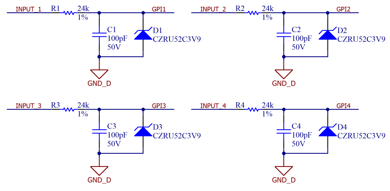
Simple solution to adapt a rather wide range of input voltages to 3.3 V levels.
Schematic
A resistor limits the current while a Zener diode saturates the voltage. EVE/CAP will detect as "low" any voltage lower than 0.8, and as "high" any voltage greater than 3 V, while still being tolerant to input voltages up to 30 V.
Signals description
Signal | Description |
|---|---|
| INPUT_1 | Digital inputs 1 to 4 |
| INPUT_2 | |
| INPUT_3 | |
| INPUT_4 | |
| GPI1 | To be connected to pin 18 (NET) or 47 (CORE) of EVE/CAP Interface connector |
| GPI2 | To be connected to pin 19 (NET) or 49 (CORE) of EVE/CAP Interface connector |
| GPI3 | To be connected to pin 20 (NET) or 53 (CORE) of EVE/CAP Interface connector |
| GPI4 | To be connected to pin 32 (NET) or 58 (CORE) of EVE/CAP Interface connector |
| GND_D | Logic supply reference voltage. To be connected to pins 15, 16 or 35 of EVE/CAP Interface connector |
Design Notes
For simplicity, the proposed solution is not opto-isolated. Therefore, the input signals generator (could be a PLC or other controller) must share the Ground with EVE/CAP.
- 24 kΩ is not a random value. It is intended to fit the voltage-current characteristic curve of the Zener diodes.
- Capacitors form a 1st order filter with the resistors. This will typically reject high-frequency noise coupled to the wiring in most of the cases.
Bill of materials
Designator | Part Number | Manufacturer | Package | Value / Description |
|---|---|---|---|---|
| R1, R2, R3, R4 | RC0603FR-0724KL | Yageo | 0603 | Thick film resistor, 24 kΩ, 1 % tolerance, 0.1 W |
| C1, C2, C3, C4 | CC0402JRNPO9BN101 | Yageo | 0402 | Ceramic capacitor, 100 pF, 50 V, NP0 |
| D1, D2, D3, D4 | CZRU52C3V9 | Comchip | 0603 | Diode Zener 150 mW 5% 0603. 3.9 V @ 5mA, 3.3 V @ 1mA |
Digital Outputs
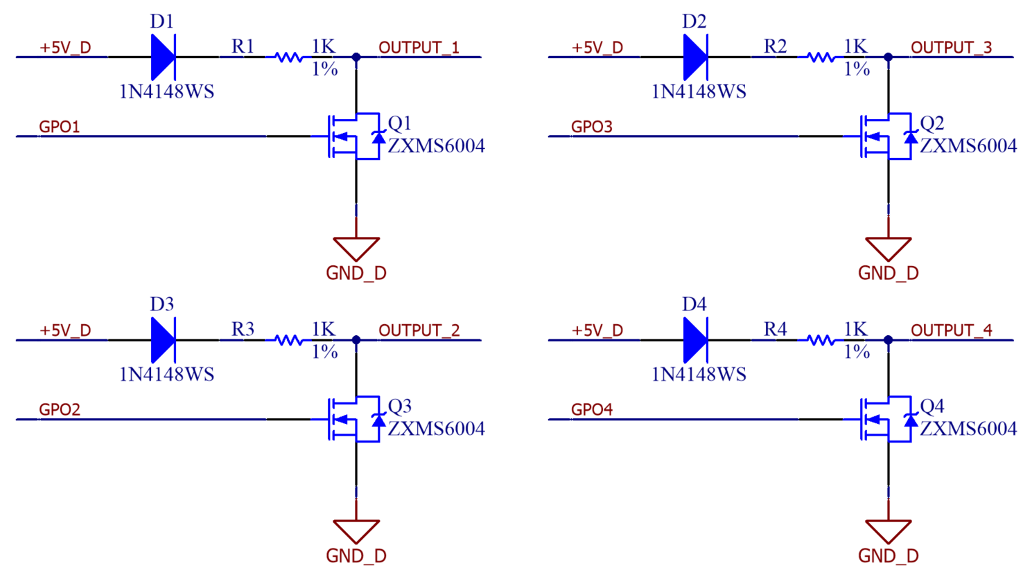
This simple circuit can be used to convert the 3.3 V push-pull digital outputs of EVE/CAP into 5 V open collector with weak pull-ups. This will invert the logic polarity of the output, but at the same time it will provide the capability of driving greater loads.
Schematic
The following circuits should allow driving loads up to 48 V and 1 A safely.
Signals description
Signal | Description |
|---|---|
| +5V_D | +5 V Logic supply |
| OUTPUT_1 | Digital outputs 1 to 4 |
| OUTPUT_2 | |
| OUTPUT_3 | |
| OUTPUT_4 | |
| GPO1 | To be connected to pin 29 (NET) or 55 (CORE) of EVE/CAP Interface connector |
| GPO2 | To be connected to pin 30 (NET) or 56 (CORE) of EVE/CAP Interface connector |
| GPO3 | To be connected to pin 31 (NET) or 57 (CORE) of EVE/CAP Interface connector |
| GPO4 | To be connected to pin 17 (NET) or 43 (CORE) of EVE/CAP Interface connector |
| GND_D | Logic supply reference voltage. To be connected to pins 15, 16 or 35 of EVE/CAP Interface connector |
Design Notes
The suggested MOSFETs do not require gate biasing.
- Also, the suggested MOSFETs feature short-circuit, overload, over-temperature and inverse polarity protection.
This solution should allow driving small inductive loads with no need of a wheeling diode.
- When driving loads in open collector configuration, only the negative terminal of the load must be connected to the output. Although it is an output, it will work by sinking current. The positive terminal of the load would be connected to a power source which Ground terminal is shared with EVE/CAP.
- When using the load in push-pull configuration, the 1 kΩ resistor set the output impedance and limit the current. In this case, note that the polarity of the GPOx signal coming from EVE/CAP will be inverted in the output.
Bill of materials
Designator | Part Number | Manufacturer | Package | Value / Description |
|---|---|---|---|---|
| D1, D2, D3, D4 | 1N4148WS | Fairchild | SOD-323F | Diode rectifier 75 V, 150 mA |
| R1, R2, R3, R4 | RMCF0402FT1K00 | Stackpole | 0402 | Thick film resistor, 1 kΩ, 1 % tolerance, 1/16 W |
| Q1, Q2, Q3, Q4 | ZXMS6004FFTA | Diodes Inc. | SOT-23F | N-channel MOSFET , 60 V, 1.3 A |
Mechanical Brake Output
Because of its similarities, the same circuit as the one proposed in the Shunt Braking Resistor Transistor section could be used. However, for cost and space optimisation, the following circuit is proposed. This would provide a 24 V tolerant open collector output for driving a mechanical brake of the solenoid type.
Schematic
Signals description
Signal | Description |
|---|---|
| BAKE+ | Positive terminal of the brake solenoid |
| BAKE- | Negative terminal of the brake solenoid |
| PWM_BRAKE | To be connected to pin 41 (NET) or 42 (CORE) of EVE/CAP Interface connector |
| GND_D | Logic supply reference voltage. To be connected to pins 38 or 46 of EVE/CAP Interface connector |
| GND_P | Power supply reference voltage. To be connected to power pin 2 of P1 in EVE/CAP |
Design Notes
- Signal BRAKE+ is to be connected to the positive terminal of the brake solenoid, and at the same time to the positive terminal of the brake power supply. The negative terminal of the brake power supply must be tied to GND_P.
- If the DC bus is supplied at 24 V or less, the signal BRAKE+ could be tied to SUP_PROTECTED or externally connected to the positive terminal of the power supply.
- The net-tie between the GND_D and the GND_P allows sharing the same reference voltage while controlling the return path in the layout phase.
- As a solenoid is a highly inductive load, the wheeling diode D1 provides a discharge path for the energy stored in it.
In case of a low voltage DC bus
EVE/CAP DC bus can be driven from a very low voltage power supply, but still a 24 V brake might be required. In the event that the DC bus is lower than the brake driving voltage, the signal BRAKE+ must not be tied to the DC bus (either SUP_PROTECTED, POW_SUP or power pin 1 of P1 in EVE/CAP). If doing so, diode D1 would short the DC bus to a greater voltage, allowing a great current through it, and most probably burning it.
Bill of materials
Designator | Part Number | Manufacturer | Package | Value / Description |
|---|---|---|---|---|
| D1 | SK310A-LTP | Micro Commercial | SMA / DO-214AC | Diode Schottky, 3 A, 100 V |
| Q1 | SSM3K324R,LF | Toshiba | SOT-23-3N | Logic-level N-Channel MOSFET, 30 V, 4 A |
| R1 | RMCF0402FT100R | Stackpole | 0402 | Thick film resistor, 100 Ω, 1 % tolerance, 1/16 W |
| R2 | RMCF0402FT10K0 | Stackpole | 0402 | Thick film resistor, 10 kΩ, 1 % tolerance, 1/16 W |
Motor Temperature Input
The EVE/CAP allows the connection of an external motor temperature sensor, typically a 2-wire sensor based on changes of resistance (PTC thermistor, bimetal, NTC, PT100, silicon temperature sensors).
Schematic
Simple but effective signal conditioning can be done with a voltage divider, a low-pass filter and a ferrite bead for decoupling.
Signals description
Signal | Description |
|---|---|
| MOTOR_TEMP_IN | Positive terminal of the external temperature sensor |
| MOTOR_TEMP_RET | Negative terminal of the external temperature sensor |
| MOTOR_TEMP | To be connected to pin 13 of EVE/CAP Feedback connector |
| +5V_D | +5 V Logic supply |
| GND_D | Logic supply reference voltage. To be connected to pins 38 or 46 of EVE/CAP Interface connector |
| GND_A | Analog reference voltage. To be connected to pins 1 or 2 of EVE/CAP Feedback connector |
Design Notes
- It is recommended to decouple the motor temperature return (MOTOR_TEMP_RET) to GND_D instead to GND_A for better EMI performance.
- A different pull-up voltage (+5V_D in the schematic) can be used, but 5V provides the maximum resolution. Pull-up voltage must be configured in the firmware register "Motor temperature voltage reference - 0x110". Further information on Summit Reference Manual, section Motor and brake.
- Pull-up resistor must be configured in the firmware register "Motor temperature external resistance - 0x10D". Further information on Summit Reference Manual, section Motor and brake
Bill of materials
Designator | Part Number | Manufacturer | Package | Value / Description |
|---|---|---|---|---|
| R1 | CPF0402B1K65E1 | TE Connectivity | 0402 | Thin film resistor, 1.65 kΩ, 0.1 % tolerance, 1/16 W |
| R2 | RMCF0402FT10K0 | Stackpole Electronics | 0402 | Thick film resistor, 10 kΩ, 1 % tolerance, 1/16 W |
| C1 | GRM155R71C104KA88D | Murata Electronics | 0402 | Ceramic capacitor, 100 nF, 16 V, X7R |
| L1 | MMZ1005S102CT000 | TDK Electronics | 0402 | Signal Line Ferrite Bead 1 kOhms @ 100MHz |
Output Supplies
3.3 V and 5 V Output Supplies
To be able of supplying external circuitry, like feedback sensors or command sources, two load switches are implemented as identical circuits. This would limit the current drawn from the outside, providing both short-circuit and overload protection, and thus maintaining the internal logic supply lines safe. Additionally, TVS diodes are added for ESD protection.
External current consumption
Both 5 V and 3.3 V internal logic supplies must be able of handling the self-consumption plus the maximum current limit set here. Otherwise the internal logic supplies could drop before the load switch overcurrent protection acts, which could cause failures of diverse nature. See Logic supply chapter above for more information.
GND connection required
External circuitry supplied this way must have its reference or Ground voltage connected to GND_D
Schematic
Signals description
Signal | Description |
|---|---|
| +5V_D | +5 V internal Logic supply |
| +3.3V_D | +3.3 V internal Logic supply |
| +5V_OUT | +5 V output supply for external circuits |
| +3.3V_OUT | +3.3 V output supply for external circuits |
| GND_D | To be connected to GND_D in the EVE/CAP Interface connector |
Design Notes
- R1 and R2 set the current limit. Considering the tolerances of both the load switch and the resistor, the current would be limited to a minimum of 246 mA and a maximum of 315 mA, with a typical value of 282 mA. Thermal drifts are not considered in this calculation.
- This approach provides a quite rugged overcurrent protection, but it is very weak in front of overvoltage. Any voltage over 6.5 V in the output might cause permanent damage to the load switch. TVS will help here, put not to become an overvoltage protection in DC.
Bill of materials
Designator | Part Number | Manufacturer | Package | Value / Description |
|---|---|---|---|---|
| C1, C2, C4, C5 | GRM155R71C104KA88D | Murata | 0402 | Ceramic capacitor, 100 nF, 16 V, X7R |
| C3, C6 | C1005X7S1A105K050BC | TDK | 0402 | Ceramic capacitor, 1 µF, 10 V, X7S |
| D1 | PTVS5V0S1UR,115 | NXP | SOD-123W | Unidirectional diode TVS, 5 V standoff, 9.2 V max. clamping, 400 W |
| D2 | PTVS3V3S1UR,115 | NXP | SOD-123W | Unidirectional diode TVS, 3.3 V standoff, 8 V max. clamping, 400 W |
| R1, R2 | RMCF0402FT100K | Stackpole | 0402 | Thick film resistor, 100 kΩ, 1 % tolerance, 1/16 W |
| U1, U2 | AP2553W6-7 | Diodes Incorporated | SOT-23-6N | 5.5 V self-protected load switch, adjustable current limit |
Communications
EVE/CAP is compatible with EtherCAT and CANopen communication protocols. An Ethernet physical layer will be required to interface the EVE/CAP through EtherCAT, while a CAN physical layer will do for CANopen. Although the EVE/CAP hardware is the same, each protocol is enabled by a different firmware, which can be freely downloaded and installed from the configuration software (see https://novantamotion.atlassian.net/wiki/spaces/SS/pages/54505739 section).
Therefore, from the 2 circuits proposed below, typically just one would be implemented.
Ethernet (physical layer for EtherCAT)
This circuit includes the required electronics and protections required to set an Ethernet physical layer according to 100BASE-T standards.
Schematic
The main component is a dual RJ-45 connector with included magnetics. Decouplings and terminations to transformers center tap is included inside its housing.
Additionally, specialised TVS provide protection in front of an ESD or surge event, the chassis of the RJ-45 connector (shorted to PE) is decouped to GND for safety and LEDs also integrated in the RJ-45 housing are driven from EVE/CAP.
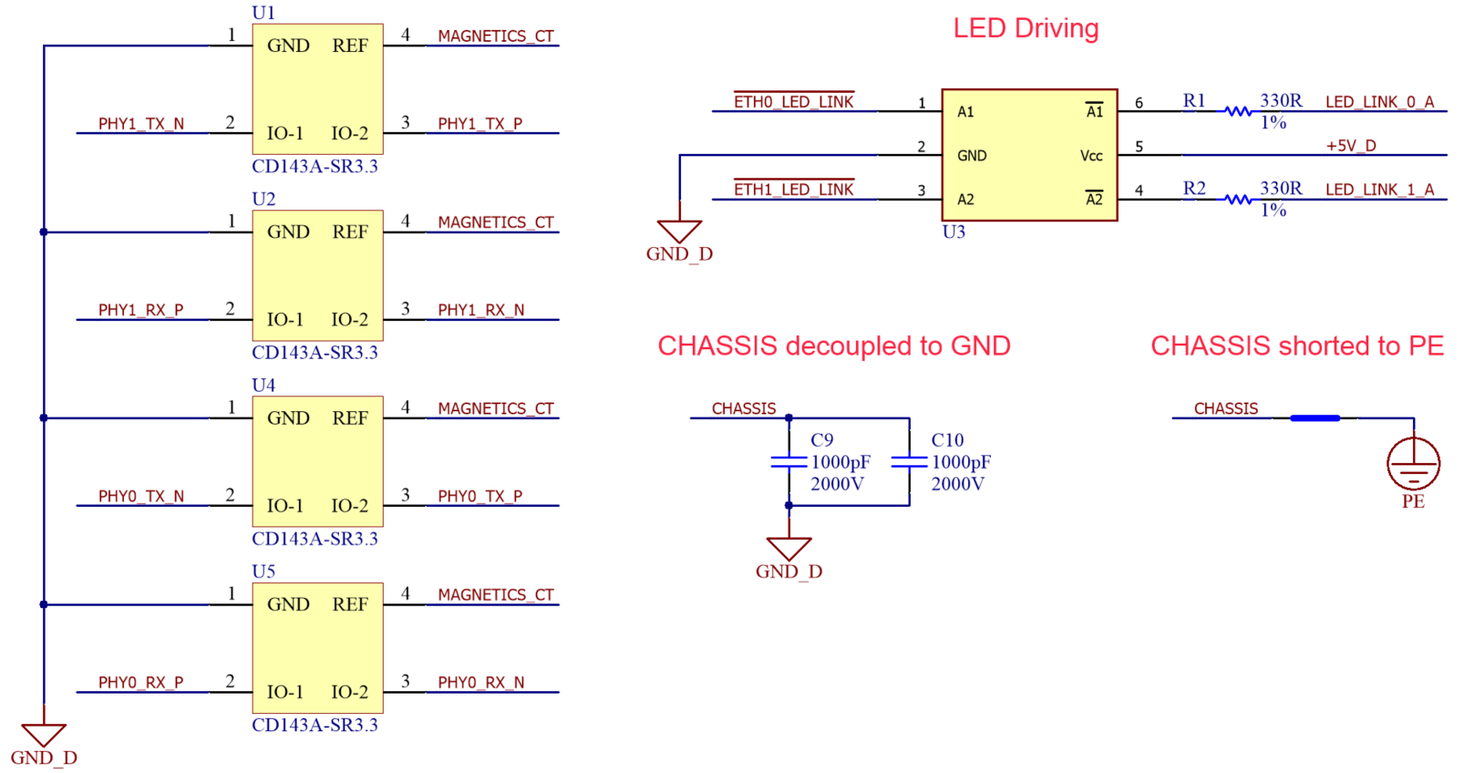
Link LED signals
Never drive an LED directly from \ETH0_LED_LINK or \ETH1_LED_LINK signals. Always use an inverting buffer. See Design Notes below.
Signals description
Signal | Description |
|---|---|
| +5V_D | +5 V Logic supply |
| MAGNETICS_CT | Center tap voltage of magnetics. To be connected to pin 13 of EVE/CAP NET Interface connector. |
| PHY0_TX_P | EtherCAT differential pairs. To be connected to pins 71 to 78 of EVE/CAP NET Interface connector |
| PHY0_TX_N | |
| PHY0_RX_P | |
| PHY0_RX_N | |
| PHY1_TX_P | |
| PHY1_TX_N | |
| PHY1_RX_P | |
| PHY1_RX_N | |
| \ETH0_LED_LINK | Ethernet Port 0 Link LED signalling. Must be buffered and inverted to drive a LED |
| LED_LINK_0_A | Anode of green LED integrated in Port 0 of the RJ-45 connector |
| \ETH1_LED_LINK | Ethernet Port 0 Link LED signalling. Must be buffered and inverted to drive a LED |
| LED_LINK_1_A | Anode of green LED integrated in Port 1 of the RJ-45 connector |
| CHASSIS | Metallic case of the RJ-45 connector |
| PE | Protective Earth |
| GND_D | Logic supply reference voltage. To be connected to pins 69, 70, 79 and 80 of EVE/CAP NET Interface connector |
Design Notes
Center tap voltage must be managed by EVE/CAP. Therefore, it must be connected to pin 13 of NET's Interface connector only, not to pin 14 and not to any other voltage source or load.
Signals \ETH0_LED_LINK and \ETH1_LED_LINK behave as configuration inputs during boot up of EVE/CAP. Therefore, this signals must always be connected to a high impedance, which means they should never drive an LED directly, but by means of an inverting buffer (U3). If this advice is not respected, the Ethernet physical layer could not work at all.
LEDs could be driven from +3.3 V instead of +5 V to simplify logic supply. However this would entail a way less stable control of the LEDs brightness.
Although TVS do not affect the basic functionality of the Ethernet physical layer, it is not recommended to remove this protection, as it is mandatory to comply with the standard.
CHASSIS may not be connected to PE (Protective Earth), as the best way to connect the CHASSIS highly depends on the electrical scenario the system will be working into.
Bill of materials
Designator | Part Number | Manufacturer | Package | Value / Description |
|---|---|---|---|---|
| C1, C3, C5, C7 | C1005X7S1A105K050BC | TDK | 0402 | Ceramic capacitor, 1 µF, 10 V, X7S |
| C2, C4, C6, C8 | GRM155R71C104KA88D | Murata | 0402 | Ceramic capacitor, 100 nF, 16 V, X7R |
| C9, C10 | 1206GC102KAT1A | AVX | 1206 | Ceramic capacitor, 1 nF, 2000 V, X7R |
| P1 | JXD0-2005NL | Pulse | RJ45 8p8c | Dual RJ45 connector with magnetics, shielded, yellow and green LEDs included |
| R1, R2 | RMCF0603FT330R | Stackpole | 0603 | Thick film resistor, 330 Ω, 1 % tolerance, 0.1 W |
| U1, U2, U4, U5 | CD143A-SR3.3 | Bourns | SOT143 | Steering / TVS diode array, 3.3 V standoff, Ethernet application-specific |
| U3 | NL27WZ14DFT2G | ON Semiconductor | SC88 / SC70-6 | Dual Schmitt trigger inverting buffer, 24 mA output, 1.65 V to 5.5 V supply |
EtherCAT / Ethernet connection between 2 drives on the same PCB
When 2 drives are mounted on the same board, many of the components needed for EtherCAT can be simplified to save space and cost. Note that there is no need for RJ45 connectors, ESD protections or high voltage capacitors.
The following schematic shows the minimal components on a board connection. Ensure the layout is differential.
Note that EVE-NET does not support capacitive coupling by default. The physical layer has auto-negotiation features enabled which becomes an issue with capacitive coupled connections. It is therefore not recommended.
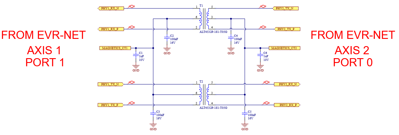
Designator | Part Number | Manufacturer | Value / Description |
|---|---|---|---|
| C1, C6 | C1005X7S1A105K050BC | TDK | Ceramic capacitor, 1 µF, 10 V, X7S |
| C2, , C3, C4, C5 | GRM155R71C104KA88D | Murata | Ceramic capacitor, 100 nF, 16 V, X7R |
| T1, T2 | ALT4532P-181-T05G | TDK Corporation | SMD LAN Transformer 180 µH 1CT:1CT |
CAN (physical layer for CANopen)
This transceiver will convert the differential levels of the CAN bus physical layer into 3.3 V levels.
Schematic
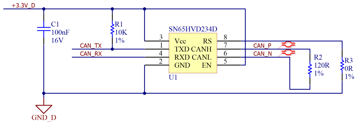
Signals description
Signal | Description |
|---|---|
| +3.3V_D | +3.3 V Logic supply |
| CAN_P | Positive terminal of CAN bus (CAN High) |
| CAN_N | Negative terminal of CAN bus (CAN Low) |
| CAN_RX | To be connected to pin 57 of EVE/CAP Interface connector |
| CAN_TX | To be connected to pin 55 of EVE/CAP Interface connector |
| GND_D | Logic supply reference voltage. To be connected to pin 59 of EVE/CAP Interface connector |
Design Notes
The design includes a termination resistor (R2), but this shall be included only in the first and last node of the bus (including the Master).
- Resistor R3 is used to limit the slope rate of the signal transition, which can have a significant impact in terms of EMC. If this becomes an issue, a value of 10 kΩ can entail a big reduction of EMI, while still being able to communicate at 1 Mbps.
- Resistor R1 is required by EVE/CAP during boot-up self-configuration.
- C1 is a decoupling capacitor for U1.
Bill of materials
Designator | Part Number | Manufacturer | Package | Value / Description |
|---|---|---|---|---|
| C1 | GRM155R71C104KA88D | Murata | 0402 | Ceramic capacitor, 100 nF, 16 V, X7R |
| R1 | RMCF0402FT10K0 | Stackpole | 0402 | Thick film resistor, 10 kΩ, 1 % tolerance, 1/16 W |
| R2 | MCHP05W4F1200T5E | Multicomp | 0805 | Thick film resistor, 120 Ω, 1 % tolerance, 1/4 W |
| R3 | MC00625W040210R | Multicomp | 0402 | Thick film resistor, 0 Ω jumper, 1/16 W |
| U1 | SN65HVD234DR | Texas Instruments | 8-SOIC | CAN transceiver, 1 Mbps |
Feedbacks
Digital Halls
This circuit assume a typical open collector output from a digital hall circuitry and provides 5 V level pull-ups to interface it. Then, a 1st order RC filter plus an Schmitt trigger buffer filter the signal and translates it to 3.3 V levels for a decent ruggedness against noise.
Schematic
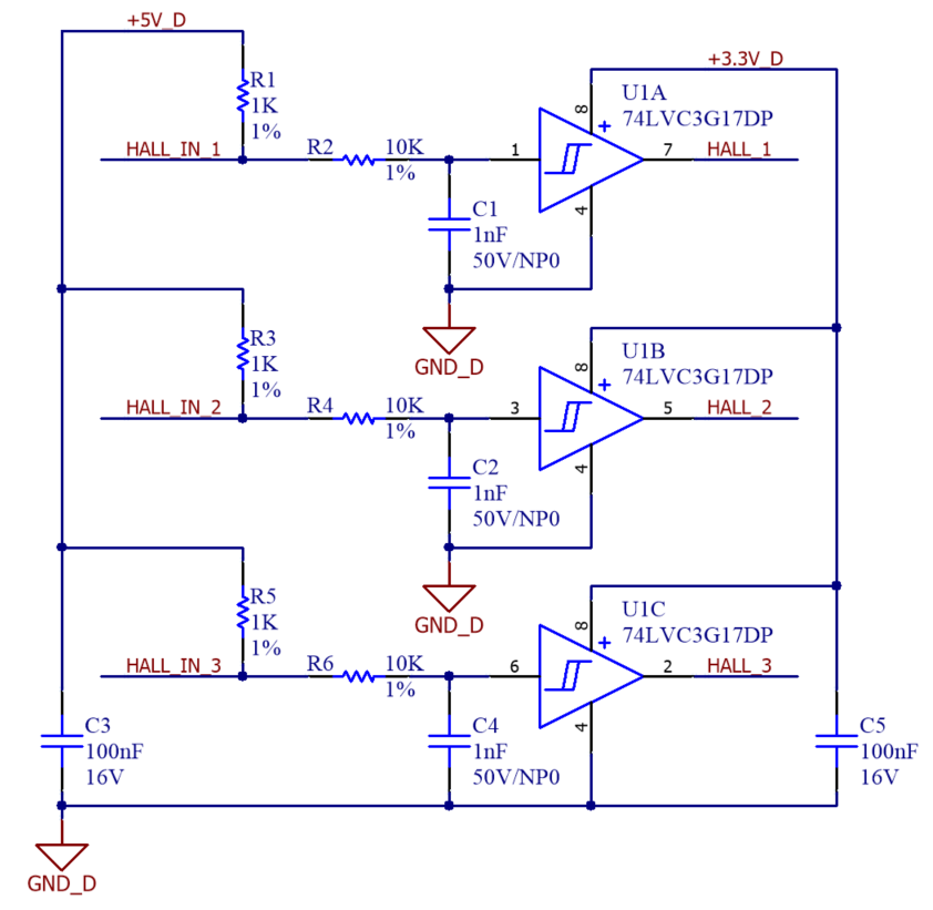
Signals description
Signal | Description |
|---|---|
| +3.3V_D | +3.3 V Logic supply |
| +5V_D | +5 V Logic supply |
| HALL_IN_1 | Digital hall inputs from motor |
| HALL_IN_2 | |
| HALL_IN_3 | |
| HALL_1 | To be connected to pins 17, 19 and 21 of EVE/CAP Feedback connector |
| HALL_1 | |
| HALL_1 | |
| GND_D | Logic supply reference voltage. To be connected to pin 15 of EVE/CAP Feedback connector |
Design Notes
- U1 is represented as 3 symbols, A, B and C, but still a single component.
- The RC filter makes a 1st order fc(-3dB) ≈ 16 kHz, but having the bandwidth of U1, the circuit should work fine with signals up to 5 kHz.
- C5 is decoupling capacitor for U1.
- U1 alone might have sufficient ESD protection.
Bill of materials
Designator | Part Number | Manufacturer | Package | Value / Description |
|---|---|---|---|---|
| C1, C2, C4 | C1005NP01H102J050BA | TDK | 0402 | Ceramic capacitor, 1 nF, 50 V, NP0 |
| C3, C5 | GRM155R71C104KA88D | Murata | 0402 | Ceramic capacitor, 100 nF, 16 V, X7R |
| R1, R3, R5 | RMCF0402FT1K00 | Stackpole | 0402 | Thick film resistor, 1 kΩ, 1 % tolerance, 1/16 W |
| R2, R4, R6 | RMCF0402FT10K0 | Stackpole | 0402 | Thick film resistor, 10 kΩ, 1 % tolerance, 1/16 W |
| U1 | 74LVC3G17DP,125 | NXP | 8-TSSOP | Non-inverting triple Schmitt trigger buffer, 24 mA output, 1.65 V to 5.5 V supply |
Differential Quadrature / Incremental Encoder
Since the inputs of the EVE/CAP are single ended 3.3 V level, signal receivers or adapters may be needed to convert differential encoder lines to single ended, filter them against noise or provide terminations or fail-safe pull-up or pull-downs.
The following circuit RS422/RS485 line receivers as hysteresis comparators. Line receivers perform very good in this kind of circuits due to its its price, high speed response, common mode tolerance and built-in ESD protection. The negative terminal is biased to 2.5 V for compatibility with single-ended encoders, while the positive terminal is pulled-up for an extra robustness in front of a weak and noisy connection.
Schematic
Signals description
Signal | Description |
|---|---|
| +3.3V_D | +3.3 V Logic supply |
| +5V_D | +5 V Logic supply |
| DIG_ENC_A | To be connected to pins 24, 26 and 28 of EVE/CAP Feedback connector to feed Incremental Encoder 1 To be connected to pins 30, 32 and 34 of EVE/CAP Feedback connector to feed Incremental Encoder 2 |
| DIG_ENC_B | |
| DIG_ENC_Z | |
| DIG_ENC_A_P | Incremental encoder channel A differential pair |
| DIG_ENC_A_N | |
| DIG_ENC_B_P | Incremental encoder channel B differential pair |
| DIG_ENC_B_N | |
| DIG_ENC_Z_P | Incremental encoder Index differential pair |
| DIG_ENC_Z_N | |
| GND_D | Logic supply reference voltage. To be connected to pin 22 of EVE/CAP Feedback connector whenever Incremental Encoder 1 is wired. Connect to pin 36 of EVE/CAP Feedback connector if Incremental Encoder 2 is wired |
Design Notes
- Resistors R3, R9 and R15 are termination resistors of a suggested 220 Ω value. Note that although 120 Ω is the recommended value for the best signal to noise-ratio on differential lines, a 120 Ω resistor tend to create unnecessary power consumption of the encoders (heating them up) and in most cases it is simply not necessary, a 220 Ω termination has empirically proven to work well for most encoders and wirings. If extra power saving was needed, consider also RC AC termination.
- C3, C4, C6, C7, C9 and C10, in combination with R4, R5, R10, R11, R16 and R17, perform a protective function of the transceiver in front of spikes or ESD, and at the same time increases immunity to common mode noise. Capacitors could be increased up to 220 pF to reinforce this effects even more if required.
- C2, C5 and C8 are decoupling capacitors for U1, U2 and U3.
- To interface a single-ended encoder, connect the ABZ signals to the positive terminal of each differential pair and leave the negative unconnected. It is mandatory that the encoder and the EVE/CAP then share their reference voltage or Ground.
Bill of materials
Designator | Part Number | Manufacturer | Package | Value / Description |
|---|---|---|---|---|
| C1, C2, C5, C8 | GRM155R71C104KA88D | Murata | 0402 | Ceramic capacitor, 100 nF, 16 V, X7R |
| C3, C4, C6, C7, C9, C10 | CC0402JRNPO9BN101 | Yageo | 0402 | Ceramic capacitor, 100 pF, 50 V, NP0 |
| R1, R2, R6, R7, R8, R12, R13, R14, R18 | RMCF0402FT2K00 | Stackpole | 0402 | Thick film resistor, 2 kΩ, 1 % tolerance, 1/16 W |
| R3, R9, R15 | ERJ3EKF2200V | Panasonic | 0603 | Thick film resistor, 220 Ω, 1 % tolerance, 0.1 W |
| R4, R5, R10, R11, R16, R17 | MC 0.063W 0603 1% 10R | Multicomp | 0603 | Thick film resistor, 10 Ω, 1 % tolerance, 1/16 W |
| U1, U2, U3 | MAX3280EAUK+T | Maxim | SOT-23-5N | Single differential RS422/RS485 line receiver, 52 Mbps, 3 V to 5.5 V supply |
Absolute Encoder
This circuit is designed to set a RS422/485-based physical layer, which is the most common among absolute encoders. It sets 2 half-duplex channels, one for the "clock" signal, which is always a transmitter driven from the EVE/CAP, and the other for the "data" signal, which is always a receiver. With this, EVE/CAP will be able to interface most SSI or BISS-C absolute encoders available.
Schematic
Signals description
Signal | Description |
|---|---|
| +3.3V_D | +3.3 V Logic supply |
| +5V_D | +5 V Logic supply |
| ABSENC_CLK_N | Clock output differential pair to absolute encoder |
| ABSENC_CLK_P | |
| ABSENC_DATA_N | Data input differential pair to absolute encoder |
| ABSENC_DATA_P | |
| ABSENC_CLK | Clock signal from EVE/CAP to be connected to pin 38 of Feedback connector or pin 24 of Interface connector |
| ABSENC_DATA | Data signal from EVE/CAP to be connected to pin 40 of Feedback connector or pin 25 of Interface connector |
| GND_D | Logic supply reference voltage. To be connected to pin 36 of Feedback connector or either pins 15, 17 or 35 of Interface connector |
Design Notes
- The circuit does not include a termination resistor the Clock output, although it might be advisable if the absolute encoder is connected along a very long cable (> 3 m), or a harsh electromagnetic environment.
- R7 is the termination resistor for the data input. In the schematic a 220 Ω resistor is suggested. Note that although 120 Ω is the recommended value for the best signal to noise-ratio on differential lines, a 120 Ω resistor tend to create unnecessary power consumption of the encoders (heating them up) and in most cases it is simply not necessary, a 220 Ω termination has empirically proven to work well for most encoders and wirings. If extra power saving was needed, consider also RC AC termination.
- C2, C3, C5 and C6, in combination with R1, R2, R6 and R8, perform a protective function of the transceiver in front of spikes or ESD, and at the same time increases immunity to common mode noise. Capacitors could be increased up to 220 pF to reinforce this effects even more if required.
- If a stronger ESD protection is required, a TVS diodes with capacitance <100 pF are acceptable, whenever C2, C3, C5 and C6 values are kept as suggested.
- The Data receiver uses a resistor voltage divider to set a 2.5 V bias. This would allow connecting this circuit to a single-ended absolute encoder and still being able to read it properly. In this case, leave the negative terminal of the differential pair unconnected.
- R4 pulls-up the positive terminal for an extra robustness in front of a weak and noisy connection.
- C1 and C4 are decoupling capacitors for U1 and U2.
Bill of materials
Designator | Part Number | Manufacturer | Package | Value / Description |
|---|---|---|---|---|
| C1, C4 | GRM155R71C104KA88D | Murata | 0402 | Ceramic capacitor, 100 nF, 16 V, X7R |
| C2, C3, C5, C6 | CC0402JRNPO9BN101 | Yageo | 0402 | Ceramic capacitor, 100 pF, 50 V, NP0 |
| R1, R2, R6, R8 | MC 0.063W 0603 1% 10R | Multicomp | 0603 | Thick film resistor, 10 Ω, 1 % tolerance, 1/16 W |
| R3 | RMCF0402FT10K0 | Stackpole | 0402 | Thick film resistor, 10 kΩ, 1 % tolerance, 1/16 W |
| R7 | ERJ3EKF2200V | Panasonic | 0603 | Thick film resistor, 220 Ω, 1 % tolerance, 0.1 W |
| R4, R5, R9 | RMCF0402FT2K00 | Stackpole | 0402 | Thick film resistor, 2 kΩ, 1 % tolerance, 1/16 W |
| U1, U2 | SN65HVD75DGKR | Texas Instruments | 8-VSSOP | RS485/422 half-duplex transceiver, 20 Mbps |
LED Signaling
EVE/CAP allows directly driving small LEDs for signaling up to 3 mA. This circuits would provide signaling for EtherCAT / CANopen status signals and Fault signaling of the internal state-machine of the EVE/CAP.
Schematic
Signals description
Signal | Description |
|---|---|
| +5V_D | +5 V Logic supply for power ON signaling |
| FAULT_SIGNAL | Fault state of the motion controller signaling. To be connected to pin 36 of the EVE/CAP Interface connector |
| ECAT_CAN_RUN | EtherCAT / CANopen "Run" status signal. To be connected to pin 65 of the EVE/CAP Interface connector |
| ECAT_CAN_ERR | EtherCAT / CANopen "Error" status signal. To be connected to pin 64 of the EVE/CAP Interface connector |
| GND_D | Logic supply reference voltage. To be connected to GND_D in the EVE/CAP Interface connector |
Design Notes
- In case brighter LEDs are required, non-inverting buffers or transistors can be used to increase the output current.
- Also, brightness might substantially vary with this solution, as 3 of the 4 signals carry 3.3 V levels. Using level shifters to 5 V, and re-dimensioning resistors R1, R2 and R3 will notably improve brightness stability.
Bill of materials
Designator | Part Number | Manufacturer | Package | Value / Description |
|---|---|---|---|---|
| R1, R2, R3 | RC0402FR-07470RL | Yageo | 0402 | Thick film resistor, 470 Ω, 1 % tolerance, 1/16 W |
| R4 | RMCF0402FT1K00 | Stackpole | 0402 | Thick film resistor, 1 kΩ, 1 % tolerance, 1/16 W |
| D1, D3 | TLMS1100-GS08 | Vishay | 0603 | Red diode LED, 63 mcd, 100 ºC |
| D2, D4 | TLMG1100-GS08 | Vishay | 0603 | Green diode LED, 35 mcd, 100 ºC |